鑫景福致力于滿足“快速服務(wù),零缺陷,輔助研發(fā)”PCBA訂購單需求。


行業(yè)新聞

PCB manufacturer's drawings describe the physICal and electrical attributes in the circuit diagram of "Gerber data file". The two documents complement each other.
Memos need to define options and exceptions
Although there are some specifications that drive the PCB design process, in these specifications, the options are almost unlimited. There are rules for everything, but almost all rules have exceptions. Defining these options and rule exceptions is part of the memo.
Explanatory memorandum: unless otherwise specified
"Unless otherwise specified" is a vague term that allows rules to casCADe hierarchically. Legal documents and contract documents are the supreme arbiters of PCB manufacturing process, followed by supporting purchase orders, and then specifIC design instructions of pyramid structure. The design notes here include manufacturing drawings and assembly drawings, which will not be repeated in this paper.
IPC-6012 defines the general precautions for rigid board manufacturing, IPC-6013 is for flexible circuit boards, and IPC-600 is a comprehensive document involving all processes. By mutual reference, dozens of standards can be applied - unless otherwise specified. Therefore, we created an illustrative memorandum to increase DFM without violating local laws, contracts and purchase orders.
1. Standards to follow:
A. Make PCB according to the current revision of IPC-6012 level 2.
B. Dimensions and tolerances shall be interpreted in accordance with the current revision of ASME Y14.5M.
C. Do not enlarge the drawing.
2. Material:
A. Tg 180 C or equivalent.
B. Equivalent materials shall comply with RoHS standards, be halogen-free, and be approved by your company.
C. The thickness of a single copper foil shall be within the range defined by the stack. See detail A.
3. Flatness:
A. The bow and warpage of the assembLED sub plate or single plate shall not exceed 0.025 mm/mm.
B. Test according to section 2.4.22 of IPC-TM-650 current version.
4. Etching geometry:
A. Measure the width on the basis of metallization.
B. Minimum line width: outer layer 0. nn mm, inner layer 0. nn mm.
C. The final line width and terminal area will not deviate from the main pattern image of 1 to 1 by+/- 0.025 mm or 20%, and the baseline is the minimum of the above two values.
5. Surface treatment: (select appropriate surface treatment (ES))
A. ChEMIcal nickel palladium plating shall be carried out according to the current revision of IPC4556. Exposed metals include 118-236 microinches of chemical nickel, 2-6 microinches of chemical palladium, and 1.2 microinches of gold.
B. Chemical gold plating shall be carried out according to the current revision of IPC-4552. The exposed metal can be selected from 118-236 μ m inch chemical nickel and 2-5 μ m inch gold.
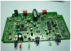
Pcb factory
6. Destructive test:
A. Some samples and reports should be provided to your design engineering department.
B. Each shipment needs to include a sample of solder used in the lead-free welding process.
C. The X-OUT panel can be used to weld samples.
7. Through hole:
A. The plating material in the hole shall be continuous electrolytic copper with a minimum thickness of 0.025 mm.
B. Minimum hole size: 0. nn mm.
C. Measure the hole size after electroplating.
D. Check the drilling chart to determine the hole size and tolerance.
E. The position of all holes shall be within 0.08 mm of the true position provided by CAD data.
8. Welding resistance layer:
A. According to the material specified in TYPE B of the current version of IPC-SM-840, the solder mask (SMOBC) is realized on the bare copper of the primary and secondary surfaces.
B. Color: matte green
C. Liquid Photoinduced (LPI) solder resist with a thickness of 0.001 mm to 0.002 mm, halogen-free
D. Leakage is not allowed on exposed SMD pads.
E. There are no exposed wires.
9. Silk screen layer:
A. The silk screen layers of the main and secondary surfaces are made of white epoxy resin and non-conductive non nutritive ink.
B. Any unspecified silk screen width shall be 0.13mm
C. Ensure that the screen printing layer does not contact any exposed metal.
D. The supplier date code, LOGO, unordered list, and any additional MARKings are on the secondary side.
10. Remove any burrs and sharp edges with radius greater than 0.003mm.
11. Non destructive assessment:
Answer: All printed circuit boards (PWBS) must pass 100% of the electrical tests defined by IPC-356 NETLIST to meet the Class 2 requirements in the revised version of IPC-9252.
B. The certificate of conformity shall be provided with each piece of goods.
12. Scrap board:
A. Scrap boards that do not meet all specifications shall be identified with permanent marks on both sides of the PCB.
B. Products without any scrap boards will be packaged together.
C. Products with n or fewer scrap boards shall be packaged separately from products without scrap boards.
D. Products with more than n scrap boards shall not be packaged.
13. PCB packaging requirements:
A. PWBS shall be packaged in vacuum sealed internal containers.
B. The external container shall be sufficient to prevent damage during transportation and handling.
14. PCB impedance (tolerance of all impedances is within plus or minus 10%)
A. The impedance of all 0.nmm wire width wires on the outer layer should be 50 ohms.
B. The differential impedance of all 0. nn mm wide/0. nn mm spaced conductor pairs on the outer layer should be 90 ohms.
C. The differential impedance of all 0. nn mm wide/0. nn mm spaced conductor pairs on the inner layer should be 90 ohms.
D. PCB suppliers can adjust PCB design geometry up to+/- 20% to achieve target impedance. Adjustment of line width, spacing or dielectric thickness exceeding 20% shall be approved by your engineering department.


抖音二維碼

Q Q二維碼

微信二維碼
點擊
然后
聯(lián)系
然后
聯(lián)系
電話熱線
13410863085Q Q

微信

- 郵箱