鑫景福致力于滿足“快速服務,零缺陷,輔助研發”PCBA訂購單需求。


行業新聞
The pcb drilling to copper is like this: the distance from the drilling edge to the nearest copper layer (pad, pouring, trace, etc.). The SMAller the drill bit, the more expensive the copper manufacturing process.
For example, as a high-performance substrate for PCB proofing, the increment of high-speed and high-frequency laminates and prepreg is the fastest. It is generally believed that at 1MHz, materials with dielectrIC constant (Dk) lower than 4 are high-speed materials. The application characteristics of high clock frequency require that Dk be as low as possible and as small as possible with temperature change.
High frequency materials are typically characterized by a dissipation factor (0,) below 0.010 at 1GHz. The proofing of circuit boards with a frequency of more than 800MHz requires that the materials have this property. Polytetrafluoroethylene (PTFE) has become the material choice for these applications.
Having a controlLED impedance means designing and producing very specific and uniform trace widths and spaces. More expensive materials with specific dielectric properties must be selected to ensure that the target electrical properties are met. Test specimens must be manufactured to ensure that the PCB manufacturer meets the 15% tolerance of the standard - sometiMES even a 5% tolerance. More work, more coupon surface area and more tests pushed up the price of the board of directors.
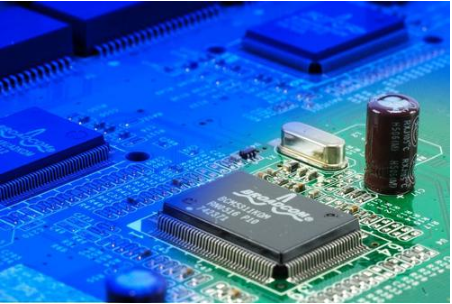
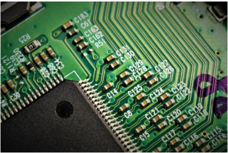
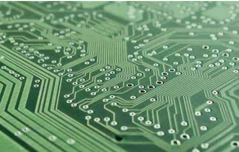
PCB proofing
Do not specify a controlled impedance unless absolutely necessary.
When you select the pcb circuit board proofing panel option, please remember that it is like the size of the circuit board: the larger the surface area, the higher your cost. Therefore, you can even pay for the waste part (faded green) thrown into the dustbin after assembly.
Mobile phone circuit board design affects audio solution
For PCB layout engineers, today's mobile phones pose the ultimate challenge. Modern mobile phones include almost all subsystems found in portable devices, such as a variety of RF modules (including cellular and short-range wireless transmission); Audio and video subsystem; Dedicated application processor and I/O layout to meet more and more application requirements, and each subsystem has conflicting requirements.
To integrate so many complex subsystems in such a small space, we should consider all kinds of realities. In addition to the possible interference between RF subsystems, the mutual interference and EMI problems between different subsystems, which may be caused by their own operation or wiring, all test the professional ability of mobile phone PCB engineers.
A well designed circuit board must be able to maximize the performance of each component mounted on it and avoid interference between different systems. Because if there are conflicts between subsystems, the performance will inevitably decline.
Today, deSPIte the increasing audio functionality in mobile phones, much attention is still focused on the RF subsystem in circuit Board Design, and the audio circuit is often the least concerned. However, audio quality, especially the characteristics of high fax audio quality, has become one of the key points that affect whether a high-end mobile phone can be quickly accepted by the MARKet. This article provides some suggestions to help ensure that a well laid out circuit board is implemented without sacrificing audio quality.
Circuit board design
1 Recommended practice for circuit board design
*Carefully consider the layout planning. The ideal layout planning should divide different types of circuits into different areas to minimize interference.
*Use differential signals whenever possible. Audio components with differential inputs can suppress noise.
*Isolate the grounding current to prevent the digital current from increasing the noise of the analog circuit.
*The analog circuit uses star grounding. The current consumption of audio power amplifiers is usually large, which may have a negative effect on their own grounding or other reference grounding.
*Turn all unused areas on the circuit board into ground plane. Perform ground floor near the signal trace, and the unwanted high-frequency energy in the signal line can be coupled to the ground through capacitance.
2 Suggested practices for PCB design
*Use hybrid circuits on the circuit board. Although the RF area of mobile phones is generally considered to be analog, the noise coupled from the RF area to the audio circuit in the circuit board design may be demodulated into audible noise.
*The analog audio signal wiring on the circuit boardis too long. Too long analog audio traces may absorb noise from digital and RF circuits.
*Forget the importance of grounding loop. A poorly grounded system is likely to suffer from serious distortion, noise, crosstalk, and low RF immunity.


抖音二維碼

Q Q二維碼

微信二維碼
點擊
然后
聯系
然后
聯系
電話熱線
13410863085Q Q

微信

- 郵箱