鑫景福致力于滿足“快速服務,零缺陷,輔助研發”PCBA訂購單需求。


行業新聞

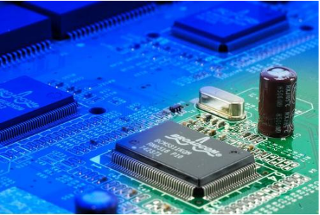
Although there are more sophistICated mounters that can replace manual welding, there are too many factors that affect the welding quality. This article will introduce several points needing attention in PCB design from the point of view of SMT welding. According to experience, if these requirements are not followed, it is likely to cause low welding quality, faulty soldering and even damage the bonding pad or circuit board when repairing PCB.
1、 Factors Affecting PCB Welding Quality
Since all components have been welded into a high quality PCB, PCB design engineers and even the level of welding process and welding workers need to be strictly controlLED. There are mainly the following factors: PCB drawing, quality of circuit board, quality of devices, oxidation degree of device pins, quality of solder paste, printing quality of solder paste, accuracy of programming of the placement machine, placement quality of the placement machine, setting of temperature curve of reflow soldering furnace, etc.
The insurmountable link of the welding plant itself is the link of PCB drawing. Because people who design circuit boards often do not weld circuit boards, they cannot obtain direct welding experience and do not know the factors that affect welding; However, the workers in the welding plant do not understand the drawing board. They just finish the production task without thinking and ability to analyze the causes of poor welding. It is difficult to organically combine these two talents because they perform their respective duties.
2、 Suggestions for PCB drawing
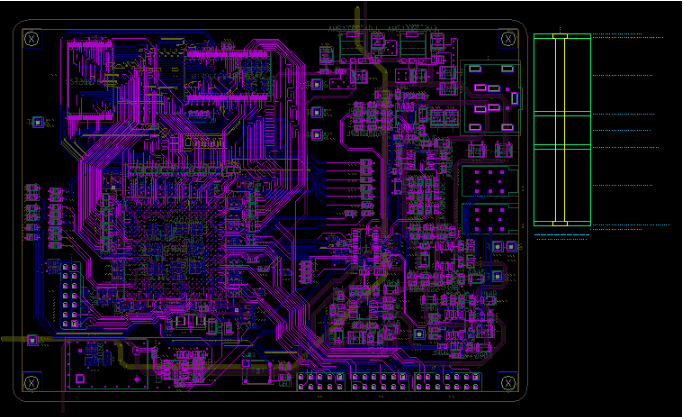
Now I will give some suggestions to the design and wiring engineers who draw PCB drawings on the link of PCB drawing, hoping to avoid various bad drawing methods that affect the welding quality in the drawing process. It will be mainly introduced in the form of pictures and texts.
1. About positioning holes: four holes (the minimum hole diameter is 2.5mm) shall be reserved at the four corners of the PCB board to position the circuit board when printing solder paste. It is required that the center of the circle in the direction of X axis or Y axis is on the same axis, as shown in the following figure:
2. MARK point: used for placement machine positioning. Mark points shall be marked on the pcb board. The specific position is: on the diagonal corner of the board, it can be round or square pads, and it shall not be mixed with pads of other devices. If there are devices on both sides, both sides should be marked.
When designing PCB, please pay attention to the following points:
a. The shape of the Mark point. (Symmetrical up and down or left and right)
b. The dimension of A is 2.0mm.
c. Within 2.0mm from the outer edge of the Mark point, there should be no shape and color changes that may cause incorrect identification. (pad, solder paste)
d. The color of the Mark point should be different from that of the surrounding PCB.
e. To ensure the identification accuracy, the surface of the Mark point is plated with copper or tin to prevent surface reflection. The shape is marked with only lines, and the light spot cannot be recognized.
3. About 5mm side: When drawing PCB, at least 3mm side shall be left in the long side direction for the chip mounter to transport the circuit board. The chip mounter cannot mount components within this range. Do not place SMD devices within this range.
For the circuit board with components on both sides, it should be considered that the PCB components on the edge of the soldered side will be rubbed off during the second reflow, and in serious cases, the bonding pad will be rubbed off and the circuit board will be damaged.
Therefore, it is recommended not to place SMD devices within 5mm from the long side of the side with few chips (usually the Bottom side). If the area of the circuit board is really limited, the edge can be processed on the long side. See Article 17 "Suggestions on the panel and the edge processing" in this paper.
4. Do not directly vialize on the bonding pad: The defect of directly vializing on the bonding pad is that the solder paste melts and flows into the vias during reflow, resulting in a lack of tin in the device bonding pad, which leads to false soldering.
5. Polarity marking of diodes and tantalum capacitors.
6. About silk screen and identification: please hide the device model. Especially the circuit board with high device density. Otherwise, dazzle will affect finding the welding position.
Don't just mark the model, not the number.
The font size of silk screen characters should not be too SMAll to see clearly. The characters shall be placed in staggered vias to avoid misreading.
7. The IC pad should be extended: the pad should be extended when drawing PCB for ic packaged by SOP, PLCC, QFP, etc. The pad length on PCB=IC foot length × 1.5 To be suitable, it is convenient to fuse the chip pin with PCB pad and tin when soldering with soldering iron manually.
8. Regarding the width of IC pad: for the IC packaged by SOP, PLCC, QFP, etc., pay attention to the width of the pad when drawing a PCB. The width of pad a on the PCB=the width of the IC foot (i.e., the Nom. value in the datasheet). Please do not increase the width, and ensure that b (i.e., between two pads) has enough width to avoid continuous welding.
9. Do not rotate the device at any angle: Since the mounter cannot rotate at any angle, it can only rotate at 90 ℃, 180 ℃, 270 ℃ and 360 ℃. As shown in Figure B below, when the placement machine rotates by 1 ℃, the device pin and the bonding pad on the circuit board will stagger by 1 ℃ after mounting, thus affecting the welding quality.
10. Problems to be noted when shorting adjacent pins: the shorting method in Figure a below is not conducive to workers' identification of whether the pins should be connected, and it will not look beautiful later. If the method in Figure b and Figure c is used for short circuit and resistance welding is added when drawing, the welding effect will be different: as long as each pin is not connected, the chip will not have short circuit, and the appearance will be beautiful.
11. With regard to the problem that there is a bonding pad in the middle of the bottom of the chip: When drawing a chip with a bonding pad in the middle of the bottom of a PCB chip, if you press the bonding pad in the middle of the chip package drawing, it is easy to cause a short circuit. It is recommended to reduce the middle pad and increase the distance between it and the surrounding pin pad, so as to reduce the chance of short circuit.


抖音二維碼

Q Q二維碼

微信二維碼
點擊
然后
聯系
然后
聯系
電話熱線
13410863085Q Q

微信

- 郵箱