鑫景福致力于滿足“快速服務(wù),零缺陷,輔助研發(fā)”PCBA訂購(gòu)單需求。


行業(yè)新聞
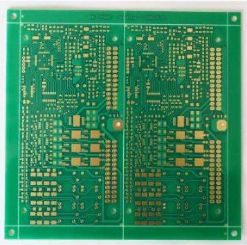
It is composed of layers of copper foil circuits. The connection between different circuit layers depends on via. This is because today's PCB manufacturing of circuit board proofing uses drilling to connect to different circuit layers. The purpose of communICation is to conduct electricity, so it is calLED through hole. In order to conduct electricity, a layer of conductive material (generally copper) must be plated on the surface of the drilling hole, In this way, PCB can move between different copper foil layers, because only the surface of the original drill hole will not conduct electricity.
PCB proofing
Generally, we often see three types of guide holes (Via), which are described as follows:
Through hole: Plating Through Hole (PTH for short)
This is the most common kind of through hole. If you just hold the PCB up against the light, the hole where you can see the light is called "through hole". This is also the SIMplest kind of hole, because when making, it is only necessary to use a drill or laser light to directly make a full hole on the circuit board, and the cost is relatively cheap. Although vias are cheap, they sometiMES use up more PCB space. For example, we have a six story house. I bought its third and fourth floors. I want to design a stair in the internal PCB that only connects the third and fourth floors. For me, the space on the fourth floor is virtually used up by the original stairs connecting the first floor to the sixth floor.
Blind hole: Blind Via Hole (BVH)
The outermost circuit of a PCB is connected to the adjacent inner layer with electroplated holes. Because the opposite side cannot be seen, it is called a "blind hole". In order to increase the space utilization of PCB circuit layers, a "blind hole" manufacturing process CAMe into being. This manufacturing method needs to pay special attention to the drilling depth (Z-axis) to be just right. You can drill holes for the circuit layers to be connected in advance at the time of individual circuit layers, and then glue them together. However, it requires more precise positioning and alignment devices. Take the purchase of a building as an example. A six story house has only a staircase connecting the first floor to the second floor, or a staircase connecting the fifth floor to the sixth floor. This is called a blind hole.
Buried Via Hole (BVH)
Any circuit layer inside the PCB is connected but not conductive to the outer layer. This manufacturing process cannot be achieved by drilling after bonding. Drilling must be performed when individual circuit layers are being drilled. The inner layer must be partially bonded first, followed by electroplating, and then all the bonding can be completed. It takes more time than the original "through holes" and "blind holes", so the price is the most expensive. This process is usually only used for high-density (HDI) circuit boards to increase the usable space of other PCB circuit layers. Take the example of buying a building above. A six storey house only has a staircase connecting the third and fourth floors, which is called a buried hole.


抖音二維碼

Q Q二維碼

微信二維碼
點(diǎn)擊
然后
聯(lián)系
然后
聯(lián)系
電話熱線
13410863085Q Q

微信

- 郵箱