鑫景福致力于滿足“快速服務,零缺陷,輔助研發(fā)”PCBA訂購單需求。


行業(yè)新聞
The invention relates to the field of circuit board manufacturing, in partICular to a nickel gold electroplating process for circuit boards.
With the development of the industry, more and more electronic products begin to use Bonding process to minimize the product volume, so more and more PCBs use nickel gold plating surface process.
In the mainstream manufacturing process, the plating process can achieve gilding at the edges of the solder joint plate, but the lead conduction solder joint and the plate edge need to be made separately, and removed after gilding, which is only applicable to gilding at the edges of the plate where the solder joint is at the edge of the plate; The nickel gold electroplating process has a SIMple production process. It does not need to make leads separately, but it can only be gilded on the top layer of the solder joint, and can not be gilded on the edge of the plate.
Plate edge gilding
Technical realization elements:
The invention provides a nickel gold electroplating process for wrapping gold on the edge of a circuit board, which can simultaneously realize gold plating on the top layer and wrapping gold on the edge of a circuit board.
To solve the above problems, as one aspect of the invention, a circuit board edge gold coated nickel gold electroplating is provided, which includes: forming an etching groove on the copper surface of the circuit board by etching, and the etching groove extends along the pattern of gold coating on the board edge to expose the side wall of the copper layer that needs gold coating; Paste a dry film on the copper layer, and form a window on the dry film. The window corresponds to the etching groove and the copper plate area enclosed by the etching groove and needs gold coating, and exposes the side wall; The circuit board is plated with nickel gold, so that a layer of nickel gold is plated on the copper plate area and the side wall.
Preferably, if the copper plate area is a separate pad, a lead is added to it separately.
Preferably, the distance between the circumferential edge of the window and the circumferential edge of the copper plate area is 4mil.
The method of the invention can simultaneously form nickel gold on the upper surface and the side wall of the copper plate area during electroplating, thereby simultaneously realizing gold plating on the top layer and gold coating on the edge of the plate.
Specific embodiments
The embodiments of the invention are described in detail below in combination with the drawings, but the invention can be implemented in a variety of different ways defined and covered by the claims.
One aspect of the invention provides a nickel gold electroplating process for gilding the edges of a circuit board, which comprises: forming an etching groove 1 on the copper surface of a circuit board by etching, and the etching groove 1 extends along the pattern of gilding the edges of the board to expose the side wall 3 of the copper layer 2 that needs to be gilded; Paste a dry film 4 on the copper layer 2, and form a window 6 on the dry film 4. The window corresponds to the etching groove 1 and the copper plate area 5 enclosed by the etching groove 1 that needs gold coating, and exposes the side wall; The circuit board is plated with nickel gold, so that a layer of nickel gold is plated on the copper plate area 5 and the side wall 3.
When making a circuit board, first, as shown in Figure 1, a layer of dry film 9 is pasted on the outer wall of copper layer 2, and a window 8 is formed on the dry film 9, which corresponds to the etching groove 1 to be formed and its shape. Then, etching is performed to form an etching groove 1. Among them, one side wall 3 of the etching groove 1 is the side wall to be side coated with gold in the subsequent process.
Then, a layer of dry film 4 is pasted on the outer wall of the copper layer 2. At the same time, a window 6 corresponding to the copper plate area 5 to be gilded on the top layer and the etching groove 1 around the copper plate area 5 to be gilded on the plate edge is formed on the dry film 4.
Finally, the circuit board is plated. At this time, the upper surface and side surface of copper plate area 5 are not covered with dry film 4, so nickel gold can be formed on the upper surface and side wall of copper plate area 5 at the same time during electroplating, so as to realize gold plating on the top layer and gold coating on the edge of the plate at the same time.
Preferably, if the copper plate area 5 is a separate pad, add a lead for it separately.
Preferably, the distance between the circumferential edge of the window 6 and the circumferential edge of the copper plate area 5 is 4 mil. In this way, it is convenient for the liquid medicine to enter the side wall of the bonding pad, and when nickel gold is plated, the plate edge is coated with gold.
Plate making process of Copper substrate
Copper substrate
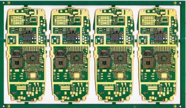
PCB is the most basic structure in the electronic industry, and the manufacturing process means the final surface treatment; That is, for example, an important means of anti-corrosion, electroplating and other treatment of copper substrate; The selection of copper substrate has a great impact on the voltage withstand, insulation resistance, dielectric constant, loss and other electrical properties, environmental protection, moisture absorption of the finished substrate;
The process technology (tin spraying) is the earliest treatment method. Its advantages are that it can be stored for a long time, low cost, and the technology is very mature. However, due to the problem of surface flatness, there are limitations in SMT. If the plate is particularly thick or thin, tin spraying has limitations, which makes it inconvenient to operate;
Electroless gold or silver plating at the same time: it is a plate shaped composite material formed by heating and pressurizing the outermost layer of copper foil, which is dissolved by some resin, dried and made into a sEMI solidified sheet, then stacked together according to the required thickness; The advantage is that the storage time is 12 months long, which is suitable for contacting and binding gold wire, and is suitable for spot testing; But the cost is relatively high, and there is also the problem of surface uniformity; We should pay more attention to the design.


抖音二維碼

Q Q二維碼

微信二維碼
點擊
然后
聯(lián)系
然后
聯(lián)系
電話熱線
13410863085Q Q

微信

- 郵箱