鑫景福致力于滿足“快速服務(wù),零缺陷,輔助研發(fā)”PCBA訂購單需求。


行業(yè)新聞
PCB has researched and developed the characteristICs of the step board, improved the development technology of the existing step board by combining the existing technology, and strengthened the step board production method. The PCB is characterized in that the PCb board method with step grooves includes the following steps: a. Paste a tape on the back of the inner core board; b. The back of the inner core plate is pasted with the first half curing sheet with a window, so that the adhesive tape is located in the window of the first half curing sheet; A second sEMI curing sheet is pasted on the front face of the inner core board; c. A first outer core plate is pasted on the surface of the first half of the curing sheet; A second outer core board is pasted on the surface of the second semi solidified sheet; d. Lamination; e. Along the direction from the second outer layer core plate to the inner layer core plate, use laser to cut along the edge of the required step groove. After cutting, take out the adhesive tape and the cut inner layer core plate, the second semi curing sheet, and the second outer layer core plate to form the one with step groove. The method of the invention can ensure that the groove wall of the step plate is neat and free of defects. After laser cutting, the laminated plate and adhesive tape can be easily taken out without sticking to the bottom of the groove. The method is SIMple, effective and convenient to implement.
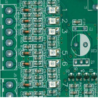
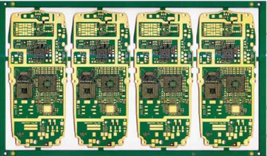
Manufacture of Mixed Dielectric PCB Multilayer
The high-frequency material selected for this manufacturing is RT/duroid 6002 plate produced by Rogers Company of the United States. This type of material is a ceramic powder filLED, glass short fiber reinforced PTFE laminate with its main properties.
Mixed media plate
Introduction to mixed medium manufacturing
The structure of the mixed medium Multilayer board
According to the design of the mixed medium multilayer plate, the production of through holes (1-16), blind holes (1-2,1-4, 13-16, 15-16) and buried holes (2-15) will be involved.
In view of the above PCB design requirements, the following route will be adopted for the production of mixed medium multilayer board reading:
(1) Template making → blanking → baking plate → punching positioning hole →
(2) One chip one pattern making → CNC drilling → brushing → plaSMA processing 1 → hole metallization → pattern transfer making 16-2 pattern → acid etching → copper sulfate etching resistance → film removal → pattern transfer making 16-2 resistance pattern → alkaline etching → film removal →
(3) Single chip two pattern transfer production 16-3 pattern → acid etching → film removal → plasma treatment 2 →
(4) Monolithic plate I and monolithic plate II are padded with prepreg plate array → laminated plate 1 → laminated plate I
(5) Single chip 3, single chip 4, single chip 5, single chip 6 pattern transfer → acid etching → film removal → black film oxidation → plate arrangement → laminate 2 → laminate 2
(6) Single chip eight making template graphics → CNC drilling → brushing → plasma treatment 3 → hole metallization → graphics transfer making 16-15 graphics → acid etching → film removal →
(7) Single chip seven pattern transfer production 16-14 pattern → acid etching → film removal →
(8) Single sheet 7, single sheet 8 plasma treatment 4 → plate arrangement → laminated 3 → laminated plate 3
(9) Laminate I fabrication of template graphics → CNC drilling → brushing → plasma treatment 5 → hole metallization → graphics transfer and fabrication of 16-4 graphics (16-1 side protection) → acid etching → film removal → plasma treatment 6 → black film oxidation →
(10) Laminate II pattern transfer production 16-5 pattern (16-12 side protection) → acid etching → film removal → pattern transfer production 16-12 pattern (16-5 side protection) → acid etching → film removal → black film oxidation →
(11) Laminated plate III making sample pattern → CNC drilling → brushing → plasma treatment 7 → hole metallization → pattern transfer making 16-13 pattern (16-16 surface protection) → acid etching → film removal → plasma treatment 8 → black film oxidation →
(12) Laminate I, Laminate II, Laminate III are padded with semi curing sheet, and then laminated → Laminate 4 → Laminate 4
(13) Laminate IV making template graphics → CNC drilling → brushing → plasma treatment 9 → concave corrosion treatment → hole metallization → graphics transfer making double-sided graphics → electrogilding → alkaline etching → double-sided depth control drilling → plasma treatment 10 → welding resistance film production → character production → contour processing → deburring → cleaning and encapsulation
It can be seen from the above PCB process flow that the processing of the mixed medium multilayer board is completed according to the board reading design requirements, and four laminating processes, five hole metallization processes, seven NC drilling operations, and ten plasma processing technologies are required before and after the processing.


抖音二維碼

Q Q二維碼

微信二維碼
點擊
然后
聯(lián)系
然后
聯(lián)系
電話熱線
13410863085Q Q

微信

- 郵箱