鑫景福致力于滿足“快速服務,零缺陷,輔助研發”PCBA訂購單需求。


行業新聞
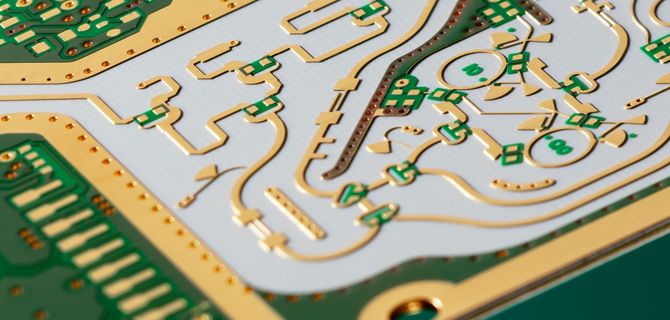
Explain four common skills in high-speed pcb design
This artICle will discuss four basic (and important) techniques and strategies for both novices and veterans. As long as you pay more attention to these skills in design, you can reduce PCB design cycle, design time and overall diagnostic difficulties
Tip 1: Pay attention to the research of manufacturing methods and foundry chEMIcal treatment process
In this era of factoriess IC companies, many engineers really do not know that the power generation steps and chemical treatment of printed circuit boards come from their design files This is not surprising This lack of practical knowLEDge often leads to more complex design choices made by novice designers, which are unnecessary For example, a mistake often made by novices is to design a layout with a particularly precise size of a printed circuit board, that is, the step of using orthogonal wires connected to a tight grid Finally, it is found that not all pcb processing plants can produce on site It is designed to maintain adequate reliability during its service life
Factories with these capabilities may not be able to provide the most economical PCB prices Does design really need to be that complicated? Can PCB layout be designed on a larger grid to reduce PCB cost and improve reliability? Other misconceptions experienced by novice designers include too SMAll through-hole sizes and blind and embedded through-hole sizes These advanced through-hole structures are printed circuit board engineers' toolkits, but their effectiveness largely depends on the specific situation Just because they are in the toolbox doesn't mean they should be used
Bert SIMonovich's "Design Notes" blog talked about the aspect ratio of vias: "The vias with an aspect ratio of 6:1 can ensure that PCB can be manufactured anywhere "For the PCB design of most high-speed vehicles, after a bit of thinking and planning, these HDI functions can be completely avoided, so as to save costs again and improve the manufacturability of the design. The physical and fluid dynamics required for these ultra small or single port through-hole copper plating are not good at all PCB factories. Recall that bad paths will destroy the entire PCB; if you have 20, 000 through-holes in your design Or you have 20, 000 chances of failure Through technology including unnecessary HDI, the probability of failure will only increase
Printed circuit board

Tip 2: Believe in the flying line
Some drawing schematics when designing a simple PCB seems to be a waste of time, especially after you have done one or two designs But for novice designers, drawing sketches can also be a difficult task Skipping the diagram is a strategy often adopted by beginners and middle level people But we must resist this strong desire Developing a layout from a complete schematic that can be used as a reference will help ensure that the layout connection is complete Some explanations are given below
First, the schematic diagram is a visual description of the circuit, which can exchange information at multiple levels The sub parts of the circuit can be drawn in detail on several pages, and components can be placed close to their functional blocks, regardless of the final physical layout Because each pin on each component is displayed in the schematic symbol, it is easy to check the soldered pin In other words, the schematic diagram helps you quickly and intuitively determine whether to follow the formal rules for describing circuits
In a set of discussions about stack overflows, A poster commented: "If the schematic diagram can mislead people to see it, it must be a bad schematic diagram. No matter what the result is, it is actually a correct schematic diagram. The problem is obvious. A technically correct but easily confused schematic diagram is still a bad schematic diagram. Although this view is easy to reach consensus, unreadable schematic diagrams can still be used in CAD programs. Expressing connection information describing circuits is still useful in layout design
The conclusion is that when designing PCB layout, having a schematic diagram as a golden reference can make the work easier Use symbols to complete the connection; When dealing with routing challenges, you do not have to consider connections at the same time Finally, I found that the wiring you forgot to perform in the first version of the design can save the number of rework
Tip 3: Use an automatic router, but don a ?? t rely entirely on the auto-router
The most professional PCB CAD tool has an automatic router But unless you are very professional in designing PCB, the automatic router will complete the wiring at one time; For PCB connection, automatic router is not a one click solution You should still know how to make manual wiring
Autorouter is a highly configurable tool In order to give full play to their role, the router parameters must be set carefully and thoughtfully for each task, and even the PCB design of each module in a single module must be set separately There is no basic general default for any occasion
When you ask an experienced designer, "What is the best automatic router?", their usual answer is "the thing between your ears (eyes)". It's not a joke. They are serious As a process, cabling is as artistic as computing; Wiring itself is heuristic. In retrOSPect, it is very similar to the traditional backtracking algorithm For constrained path selection applications (such as mazes and puzzles), backtracking algorithm is very suitable For finding answers, but it is not good at finding the optimal solution under the open and unrestricted conditions, such as printing printed circuit boards with pre arranged components Unless the designer has made a highly detailed adjustment to the constraints of the automatic router, the results of the automatic router still need to be manually checked for weaknesses in the backtracking results
Wire size is another difficulty The automatic router cannot reliably determine how much current will flow through the wire. In this case, it cannot help you determine the use width of the wire Therefore, the wire width laid by most automatic routers does not meet the requirements Many automatic routers allow you to specify reference wire constraints In the forum post on stackeexchange Every board I make has used an automatic router (sorry, it is a very high-end router) If the constraint is similar to this: only on this layer, the two signals form a differential pair, and the nets must match the length, then you must tell the auto mechanic about these conditions "When you want to use the automatic connector, you must ask yourself:" When I set the constraints of the automatic router, the PCB can even set the constraints for each wire in the schematic diagram. How many manual connections will be completed this time“
Experienced designers put a lot of energy on the initial component layout, and most half of the entire design time is spent on optimizing the component layout:
Simplified wiring minimize the crossing of flying wires, etc;
Devices are close-shorter routing means better wiring;
Signal timing considerations.
In the user forum, a post said, "Pay more attention to the Layout of components. Layout of components takes up 70% of the total workload. Before layout, place the first wire. All components use flying leads (these lines indicate the connection relationship that has not been completed yet) as a rough guide to the integrity of the wiring“
The old generation often used mixed methods for wiring hand lay some important key lines Then the automatic router is used to handle non critical routes and help manage the "escape state" in the routing algorithm This method is sometiMES a good compromise between controlled manual wiring and fast automatic wiring
Tip 4: PCB geometry and current
Most people who work in electronIC design know that This has been directly applied to the design of automobile fuses By controlling the thickness and shape of the wire (U-shaped bending, V-shaped bending, S-shaped, etc.), when overloaded, the calibration fuse will blow at the throat point The problem is that PCB designers routinely produce similar electrical that points in their PCB design For example, if you use a 90 degree elbow, two quick 45s can form an angle; Bend more than 90 degrees to form a zigzag In the best case, these wires will reduce the speed of signal transmission; In the worst case, they will explode at the resistance point, just like automobile fuses


抖音二維碼

Q Q二維碼

微信二維碼
點擊
然后
聯系
然后
聯系
電話熱線
13410863085Q Q

微信

- 郵箱