鑫景福致力于滿足“快速服務(wù),零缺陷,輔助研發(fā)”PCBA訂購單需求。


行業(yè)新聞

Improved production process of ladder circuit board
The improved step PCB production process is characterized in that it includes an upper substrate, at least one intermediate substrate and one lower substrate The process flow is as follows: (1) Cutting: the upper substrate Need to be cut to size; (2) Inner layer: the lower surface of the upper substrate, the upper surface of the lower substrate and the front and back of the intermediate substrate form a circuit pattern through image transfer, and then the unnecessary part of the copper foot is processed by a milling machine Removal to form the required loop pattern; then use a molding machine to fish the middle substitute to create a window corresponding to the position and size on the middle substitute; (3) once drilling: the upper substrate, the middle substrate and the lower substrate Aligning pin holes are drilLED on the substrate; (4) Resin printing: The alignment pin holes drilled on the upper, middle and lower substrates are selectively plugged with resin by printing; (5) Pressing: in Place the film between the upper substitute and the middle substitute and between the middle substitute and the lower substitute and stack them one by one, and send them into a vacuum locator to hard and bond the films together to form a multilayer PCB;
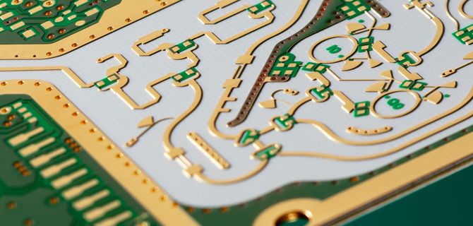
Multilayer PCB

Then, the upper surface circuit pattern of the lower substrate is exposed by the molding machine at a fixed depth at the position where the steps need to be performed; (6) Secondary drilling: Drilling on the multilayer PCB by using different specifICations of slot cutters Slot holes of the required size; (7) Plating: Copper is printed on the outer surface of the multilayer PCB through chEMIcal reaction in the tank, so that the slots can conduct between the layers; (8) Dry film: Cover a layer of dry film on the outer surface of the cop, and form a circuit image on the outer surface of the cop through image transfer; (9) Alkaline, etc; (10) Solder protection: a layer of ink is covered on the outer surface of the multilayer PCB by printing; (11) Printing: on the multilayer PCB by printing Corresponding symbols are printed on the outer surface; (12) Forming: The whole piece of multilayer PCB board is deleted from the useless frame, cleaned chemically, and classified into the specified shape and specification
Know the foundry you are using
After discussing DRC settings, this technology is almost redundant, but not completely redundant In addition to helping you formulate DRC rules correctly, knowing which foundry your PCB will be sent to can also provide some additional pre manufacturing assistance A good foundry will provide some useful help and suggestions before you place an order, including how to improve the design to reduce design iteration, reduce problems encountered in final debugging on the test bench, and improve PCBs
Hugo, PhD candidate, Carnegie Mellon University, In his blog, he commented on his understanding of manufacturers: "Each manufacturer has its own specifications, such as the minimum wire width, spacing, and number of layers. Before ETC starts designing, you should consider your own requirements, and then find a manufacturer that can meet your requirements. Your requirements also include PCB information. Grade PCB information ranges from FR-1 (paper generic resin mixture) to FR-5 (glass fiber and ring) . Oxygen resin). Most PCB Prototype manufacturers use FR-4, but FR-2 is also often used in mass consumption applications The data type will affect the strength, durability, resistance and flame tolerance of the PCB (FR)“
Understanding the manufacturing process of printed PCB and knowing which process and method your manufacturer will use can help you make better design decisions. Visit the supplier you choose to understand your manufacturing process Make good use of DFM (design for manufacturability) tools before submitting your design to manufacturing.
Summary of this article
If you are thinking about these basic skills and techniques Understand the manufacturing process; Use DRC and DFM to help you catch the possible increase in casting costs and/or decrease in production Then carefully plan the Layout of components to eliminate expensive design functions Use all the design tools provided by CAD tools wisely, including automatic layout and automatic routing. However, in order to obtain a good automatic routing effect, you must set up the automatic routing device patiently and thoroughly
Do not rely on automatic routers except for cabling; If necessary, manually adjust the wire size to ensure that the design carries the correct current In any case, you must believe in flight clues until all flight clues disappear 100%. Your PCB design can be considered complete The latter can save more time and labor in PCB proofing and PCB production
How to Solve Problems in PCB Production
11-13,2022


抖音二維碼

Q Q二維碼

微信二維碼
點擊
然后
聯(lián)系
然后
聯(lián)系
電話熱線
13410863085Q Q

微信

- 郵箱