鑫景福致力于滿足“快速服務,零缺陷,輔助研發”PCBA訂購單需求。


行業新聞

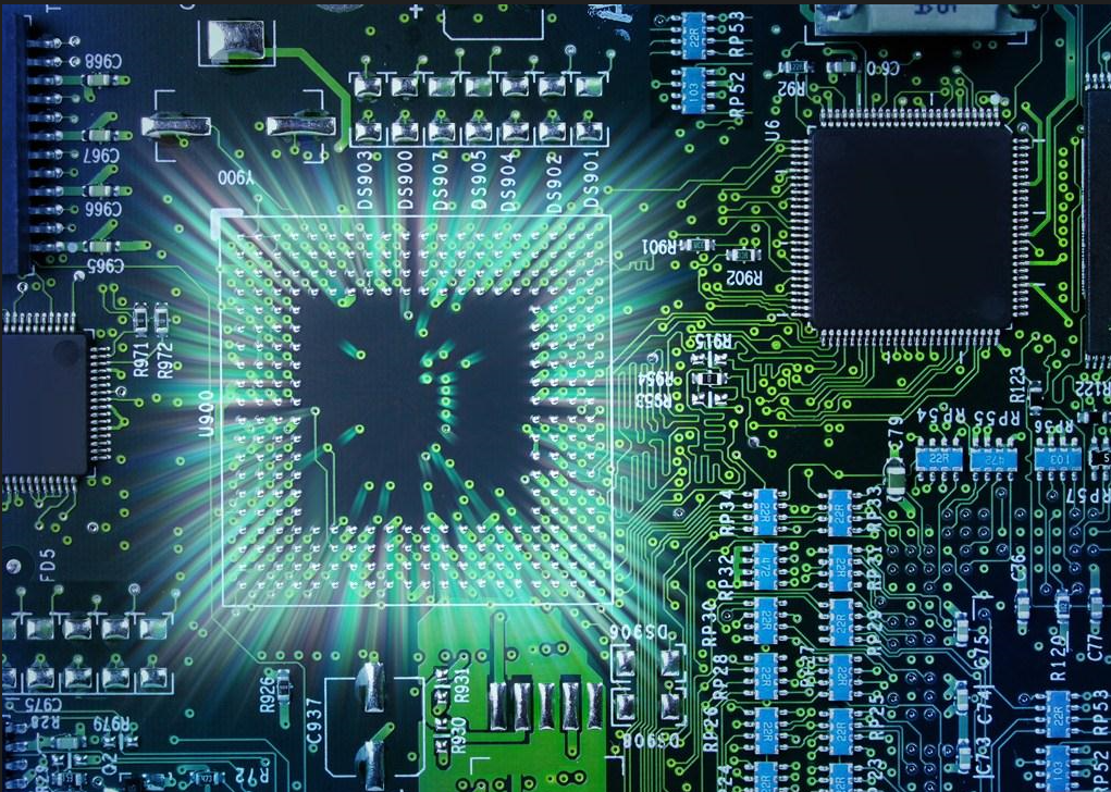
production process of PCB Single Layer, Two Layer and Multilayer
Function of PCB The functional printed circuit board (PCB) is the basis for completing the primary assembly of components and other necessary electronIC circuit board parts to form modules or finished products with specific functions Therefore, in the whole electronic product, this printed circuit board plays a role in integrating and connecting all functions of components Therefore, when electronic products fail, the first problem is usually the printed circuit board
The evolution of PCB 1 as early as 1903, sir Albert Hansen took the lead in applying the concept of "circuit" to telephone switching systems It is cut into circuit conductors with metal foil, and then pasted on paraffin paper, which is also pasted with a layer of paraffin paper. It has become the current printed circuit board mechanism By 1936, Dr. Paul Eisner had truly invented the technology and issued a number of patents Today's print wait h (photo image transfer) technology is inherited from its invention
The types and manufacturing methods of printed circuit boards are diversified in terms of materials, levels and production processes to adapt to different electronic products and their special needs.
Printed circuit board double-sided board

Cutting, drilling, copper plating, plate surface electroplating, pattern transfer, pattern electroplating, etching, quality inspection, printing solder mask (green oil/white characters), immersion gold, tin spraying, gold plating, V-shaped cutting gongs, brewery testing, FQC packaging, finished product warehouse delivery
Printed circuit board Multilayer board
Cutting Inner layer DF AOI Browning Press plate Drilling room Immersion coupler Plate plating Outer layer Etching QC11 Green oil
PCB
Printing ink (screen printing ink has different MEShes, generally 77T or 57T)
Pre-baked (different ink parameters are different, generally 75-80 degrees)
Exposure (exposure energy level 10-12)
Development (55% development point)
Visual inspection-
Post curing (150 degrees 60 minutes)
This PCB production process is divided into several aspects, including single board process, double-sided board process and multilayer board process In addition to ordinary cardboard, flexible board is also a flexible board Flexible circuit board There are still several processes, That is, single-layer flexible circuit board, multi-layer flexible circuit board, etc
Sometimes we think PCB is a very complicated thing Here is a fuzzy production process analysis of PCB First of all, we need to understand the function and function of printed circuit board The first step is to provide the basis for completing the first level assembly and other necessary electronic circuit parts to form modules or finished products with specific functions Therefore, in the whole electronic products, almost all types of electronic equipment come from electronic watches, computers, communication electronic equipment, and finally military weapon systems As long as electronIC components such as integrated circuits are used for power interconnection between them, they will be used
In the production process, printed circuit boards are generally divided into three types: single-sided, double-sided and multilayer boards Factories with different production processes are calLED different factories, but the principle of process flow is the same!
The one-sided production process is easier to understand than the two-sided production process In general, it is cut, drilled, patterned, transferred, etched, welded, masked, and printed metal surface treated, finished, molded, tested, packaged, and shipped
The whole process of double-sided plate production is: cutting, drilling, electroless copper plating and copper plating pattern transfer pattern electroplating and protective tin etching, intermediate inspection, solder mask - printed word metal surface treatment, finished product molding, electric power test, visual inspection, packaging and shipping
The multilayer PCB process is to increase the inner layer process before the double sided process Basic process: cut the inner layer pattern, transfer the inner layer etching, inner layer etching, check the copper surface oxidation treatment, typesetting, and laminate cutting plate, and then conduct the double-sided plate process after forming
The above is a printed circuit board The PCB has developed from single layer to double-sided multilayer board, maintaining their own development trend Because it has been developing in the direction of high-precision and high-density, continuously reducing the volume, reducing the cost, and better using the printed circuit board in the future development of electronic equipment, it will continue to have strong vitality
The above is the explanation given by the editor of pcb circuit board company.
If you want to know more about PCBA, you can go to our company's home page to learn about it.
In addition, our company also sells various circuit boards,
High Frequency Circuit Board and SMT chip are waiting for your presence again.


抖音二維碼

Q Q二維碼

微信二維碼
點擊
然后
聯系
然后
聯系
電話熱線
13410863085Q Q

微信

- 郵箱