鑫景福致力于滿足“快速服務,零缺陷,輔助研發”PCBA訂購單需求。


行業新聞
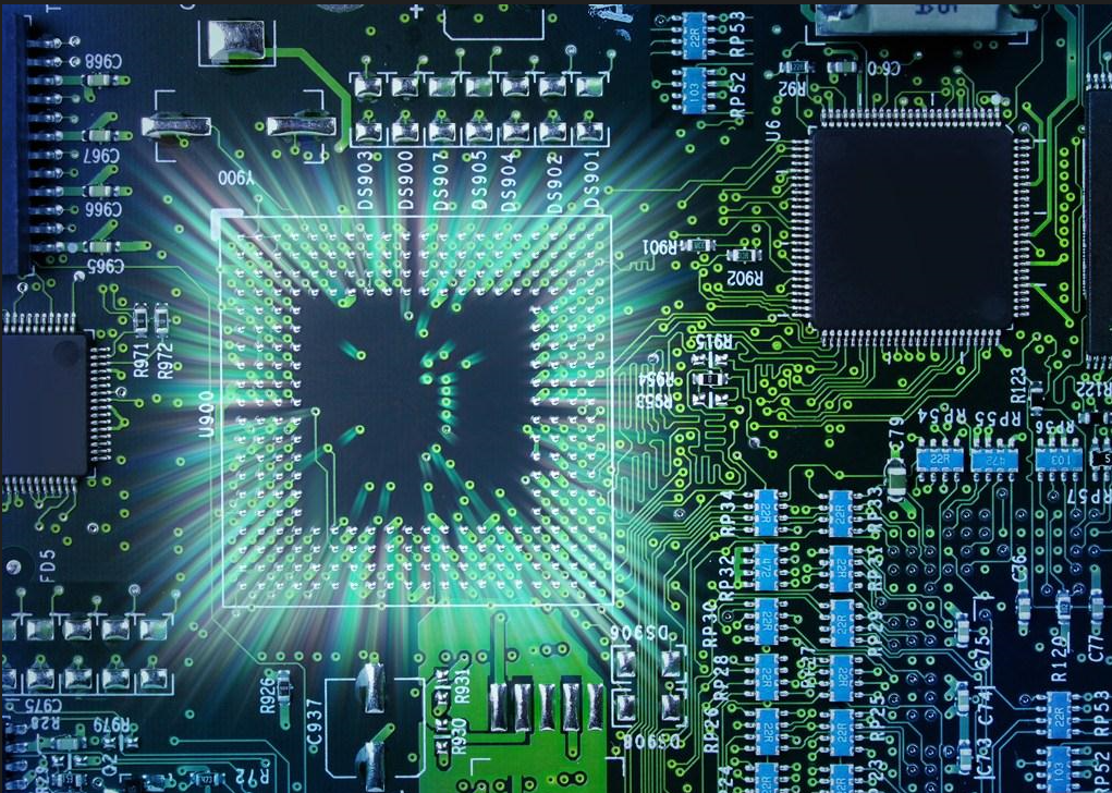
How to Solve Problems in PCB Production
In the production process, PCB board,
First, the CAM data generated by PCB CAD must be transferred to the PCB manufacturer This PCB manufacturer uses the CAM 1 data editor to check and edit film data, hole data, etc
Add reference MARKs, correction values, etc Or execute the data synthesis PCB required for production For example, check whether the distance between the pad and the aperture is reasonable
The pads are usually tin plated. The insertion hole is hollow It can be seen from the PCB design that the mat is annular
Manufacturer of PCB board

The design process of several tenths of millimeter PCB is normal, but in fact, manufacturer s needs to have a minimum width standard, and the width design is too SMAll to complete Above the usual design standards, the actual production standard PCB manufacturers need to calibrate the design standards
PCB production process
For example, the minimum width of the backing plate is 0.2 mm for some manufacturers and 0.25 mm for others If 0. 2 mm is required, the formation of the gasket cannot be guaranteed For example, 2, check the distance between the open window on the welding mask and the pad
Normally, a PCB board with a layer of green film texture on its surface is a soldering mask As the name implies, the solder mask cannot be welded normally
The window of the solder mask is usually designed to be larger than the diameter of the pad This is to keep a certain distance between the window and the mat
It is usually set to 0.2mm. In this case, even if some error occurs on the circuit board, the solder mask will not cover the pad, resulting in poor welding Example 3: Check the minimum width and minimum spacing of traces The usual procedure can achieve the minimum width and minimum spacing of 0 2mm, respectively When it is small, special processes are required Only the minimum standard manufacturers describe what can be achieved under normal conditions Example 4: Check the minimum distance between edges PCB board or the non tin placed through hole (NPTH) and the trace
The minimum distance between edges of PCB board and the trace is normally set to 1mm (0.5mm (if necessary), not recommended) to prevent the trace from being split when the PCB board is divided
Set to 3mm When using the machine to weld components to PCB boards, due to the limitations of the actual machine itself, it can avoid damaging PCB boards with traces near the edges
The contour PCB assembly (indICated by silkscreen) is usually kept at a distance of more than 1mm from the edge of the PCB (except for the parts at the specified position in the design)
The pad and PCB of the assembly shall be kept at least 1mm, usually 3mm to 5mm In addition to preventing cracking, it can also reduce the fatigue of the gasket and prevent the gasket from falling off the support due to the relative stress of PCB
The minimum distance between non-tinned holes (NPTH) and traces is determined by the use of non-tinned holes.
Normally, the distance between the component through hole and the trace is normally set to 1mm or more (if necessary, it can be set to 0.5mm, not recommended), M3 screw hole. Generally, it is prohibited to wire within 10mm in diameter and place components prevent metal screw contact trace and short circuit
Note: The above minimum settings are PCB boards, not cam settings All of the above checks can be performed automatically by setting the cam 3 When the inspection and correction work is completed, the data of various processing equipment can be generated
Remark:
1. CAM: Computer Aided Manufacturing
2. The PCB design mentioned here is the most unwritten standard in the industry, which I described in the design Readers need to refer to PCB manufacturers to formulate their own design standards in PCB design
The old people speak very well. You can't beat around the bush without rules
The above is the explanation given by the editor of pcb circuit board company.
If you want to know more about PCBA, you can go to our company's home page to learn about it.
In addition, our company also sells various circuit boards,
High Frequency Circuit Board and SMT chip are waiting for your presence again.


抖音二維碼

Q Q二維碼

微信二維碼
點擊
然后
聯系
然后
聯系
電話熱線
13410863085Q Q

微信

- 郵箱