鑫景福致力于滿足“快速服務,零缺陷,輔助研發”PCBA訂購單需求。


行業新聞
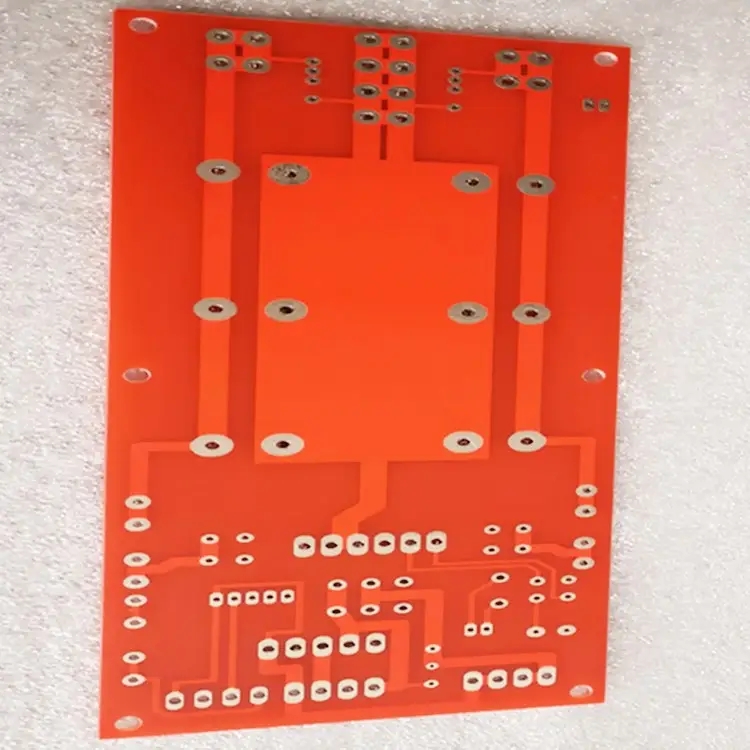
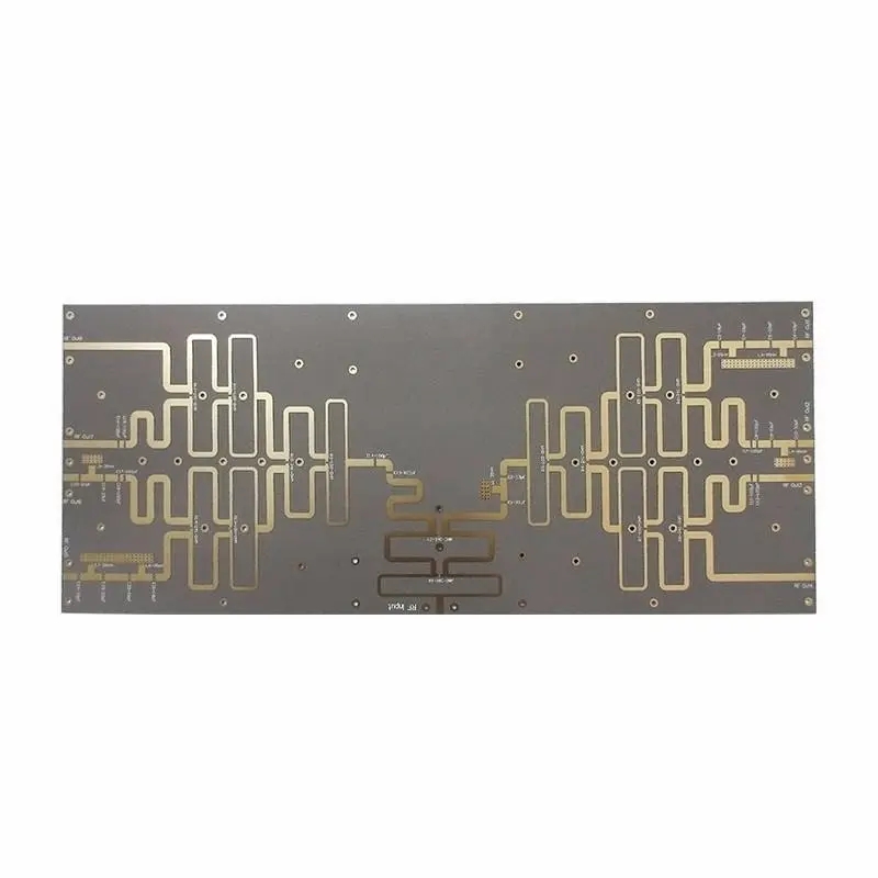
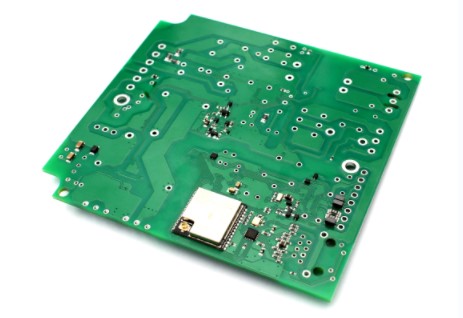
On the layout of PCB components and what is PCB made of?
During PCB layout, after the system layout is completed, the PCB drawing shall be reviewed to see whether the system layout is reasonable and can achieve the optimal effect. Generally, the following aspects can be considered:
Whether the system layout can ensure the reasonable or optimal wiring, whether it can ensure the reliable wiring, and whether it can ensure the reliability of circuit work. In the layout, it is necessary to have an overall understanding and planning of the signal direction and the power and ground network.
2. Whether the size of the printed board is consistent with the size of the processing drawing, whether it meets the requirements of PCB manufacturing process, and whether it has behavior MARKs. This requires special attention. The circuit layout and wiring of many PCB boards are designed beautifully and reasonably, but the precise positioning of the positioning connector is neglected, whICh makes the designed circuit unable to connect with other circuits.
3. Whether the components have conflicts in 2D and 3D space. Pay attention to the actual size of the device, especially the height of the device. The height of components without layout in welding shall not exceed 3mm generally.
4. Whether the Layout of components is dense, orderly and orderly, and whether they are completely distributed. In the layout of components, it is not only necessary to consider the direction and type of signals, places needing attention or protection, but also the overall density of component layout to achieve uniform density.
5. Whether the components that need to be replaced frequently can be easily replaced, and whether the plug-in board can be easily inserted into the equipment. The replacement and connection of frequently replaced components shall be convenient and reliable.
6. Whether it is convenient to adjust the adjustable elements.
7. Whether there is an appropriate distance between the thermal element and the heating element.
8. Whether radiator or fan is instalLED at the place where heat dissipation is required, and whether the air flow is smooth. Attention shall be paid to the heat dissipation of components and circuit boards.
9. Whether the signal direction is smooth and the interconnection is shortest.
10. Whether plugs, sockets, etc. contradict with mechanical design.
11. Whether the interference of lines has been considered.
12. Whether the mechanical strength and performance of the circuit board have been considered.
13. The artistry and aesthetics of circuit board layout.
What is PCB made of?
printed circuit board materials are glass fiber/plastic substrate, solder mask, copper and naming ink.
Plastic substrate/glass fiber
Manufacturers can use flexible or rigid surfaces when manufacturing PCBs. These two surfaces depend entirely on the PCB design required for the project. Importantly, a tough surface requires polyamide glass fiber or FR4. At the same time, high temperature polyamide film and other flexible materials are used for the flexible surface. Some common non-conductive substrates for flexible panels include polyamides, liquid crystal polymers, polyethylene, and polyesters. In addition, these substrates provide a non-conductive surface on which all conductive circuits operate.
Copper wire has very high conductivity. The plastic substrate used is laminated with thin copper traces on all plastic surfaces. However, for multilayer PCB, the structure is different. The multilayer has alternating copper layers, which act as a conductive material of the insulating material.
Solder mask
Solder resist layer is a kind of fluid, which is usually applied to the outer layer of rigid printed circuit board. Importantly, its job is to cover copper sheets to prevent them from oxidation. In addition, when all components are on the board, the fluid retains and controls the flow of molten solder. When the liquid solder flows out of the surface, it is possible to connect two adjacent circuits to form a short circuit. It is worth noting that the solder resist has a typical green color. However, you can also use other colors, such as blue, white, red, and transparent.
After applying the solder mask, the next step is to print the barcode, identification information and marks. These tags are nomenclature. Crucially, jargon helps to achieve accurate PCB assembly.
PCB manufacturing, PCB design and PCBA processing manufacturers will explain to you the layout of PCB components and what PCB is made of?


抖音二維碼

Q Q二維碼

微信二維碼
點擊
然后
聯系
然后
聯系
電話熱線
13410863085Q Q

微信

- 郵箱