鑫景福致力于滿足“快速服務,零缺陷,輔助研發”PCBA訂購單需求。


行業新聞
The circuit board manufacturer explains where the crystal oscillator is placed?
PCB manufacturers, PCB designers and PCBA manufacturers explain the placement of crystal oscillators for you?
Some Electronic devices need AC signals with highly stable frequency, while LC oscillators have poor stability and are easy to drift (that is, the frequency of the generated AC signal is easy to change). In the oscillator, a special element - quartz crystal is used to generate a highly stable signal. This oscillator using quartz crystal is calLED a crystal oscillator.
The crystal oscillator has the piezoelectrIC effect, that is, the crystal will deform after the applied voltage at the two poles of the chip. In turn, if the external force deforms the chip, the metal chips at the two poles will generate voltage. If an appropriate alternating voltage is applied to the chip, the chip will resonate (the resonant frequency is related to the tilt angle of the quartz slope, and the frequency is certain). Crystal oscillator is a kind of crystal that can convert electrical energy and mechanical energy into each other. It can provide stable and accurate single frequency oscillation when working in resonance state. Under normal working conditions, the absolute accuracy of ordinary crystal frequency can reach 50 parts per million. Using this characteristic, crystal oscillator can provide more stable pulse, which is widely used in the clock circuit of microchip. The wafers are mostly quartz semiconductor materials, and the shell is metal encapsulated.
The crystal oscillator is often connected with the main board, south bridge, sound card and other circuits. The crystal oscillator can be likened to the "heartbeat" generator of each board. If the "heartbeat" of the main card goes wrong, other circuits will fail.
1. Radiation source analysis
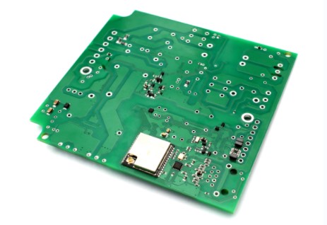
The PCB has a 12MHz crystal. Among them, the frequency points exceeding the standard are all 12MHz frequency multiples. Through analysis of the screen and CAMera prone to EMI radiation exceeding the standard, it is found that LCD-CLK is 33MHz, while camera MCLK is 24MHz.
Through the elimination method, it is found that after the camera is removed, the superscript point still exists, while by shielding the 12MHz crystal, the superscript point is reduced, so it is judged that the 144MHz superscript point is related to the crystal. The PCB layout is as follows:
2. Radiation generation principle
It can be seen from the PCB layout that the 12MHz crystal is just arranged on the edge of the PCB. When the product is placed in the radiation emission test environment, the high-speed components of the product under test will form a certain capacitive coupling with the reference ground in the laboratory, generating parasitic capacitance, resulting in common mode radiation. The larger the parasitic capacitance, the stronger the common mode radiation; The parasitic capacitance is essentially the electric field distribution between the crystal and the reference ground. When the voltage between the two is constant, the more electric field distribution between the two, the greater the electric field strength between the two, and the larger the parasitic capacitance. When the crystal is at the edge of the PCB and in the middle of the PCB, the electric field distribution is as follows:
When the crystal oscillator is arranged in the middle of the PCB or far away from the edge of the PCB, due to the existence of the working ground (GND) plane in the PCB, most of the electric field is controlled between the crystal oscillator and the working ground, that is, in the PCB, the electric field distributed to the reference ground plate is greatly reduced, leading to the reduction of radiation emissions.
3. Treatment measures
Move the crystal oscillator inward so that it is at least 1cm away from the PCB edge, and lay copper on the PCB surface layer within 1cm away from the crystal oscillator. At the same time, connect the copper on the surface layer with the PCB ground plane through the via.
4. Thinking and enlightenment
The capacitive coupling between high-speed printed lines or devices and the reference ground plate will cause EMI problems, and the placement of sensitive printed lines or devices on the edge of PCB will cause interference immunity problems. If it must be arranged on the edge of PCB for other reasons in the design, then another working ground wire can be laid on the edge of the printed line, and more vias can be added to connect the working ground wire with the working ground plane.
PCB manufacturers, PCB designers and PCBA manufacturers explain the placement of crystal oscillators for you?


抖音二維碼

Q Q二維碼

微信二維碼
點擊
然后
聯系
然后
聯系
電話熱線
13410863085Q Q

微信

- 郵箱