鑫景福致力于滿足“快速服務(wù),零缺陷,輔助研發(fā)”PCBA訂購(gòu)單需求。


行業(yè)新聞

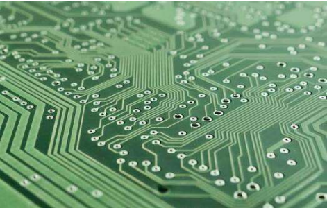
We often encounter the problem of windowing. Now let's follow the PCB proofing manufacturer to learn about the windowing design of PCB design.
TOP/BOTTOM SOLDER. The welding pad, through hole and the non electrICal wiring of this layer shall be welded with green oil to open the window.
By default, the bonding pad will open a window in PCB design (OVERRIDE: 0.1016mm), that is, the bonding pad will expose copper foil, expand 0.1016mm, and tin will be applied during wave soldering. No design change is recommended to ensure weldability;
2. In PCB design, via will be windowed by default (OVERRIDE: 0.1016mm), that is, via will expose copper foil, expand 0.1016mm, and tin will be applied during wave soldering. If it is designed to prevent the vias from being tinned and copper exposed, the PENTING option in SOLDER MASK, the additional attribute of the vias, must be checked to close the vias.
3. In addition, non electrical wiring can also be conducted on this layer separately, so the green oil of resistance welding shall be opened accordingly. If it is on the copper foil wiring, it is used to enhance the over-current capacity of wiring, and tin is added during welding; If it is on the non copper foil wiring, it is generally designed to be used for identification and special character silk screen printing, which can save the production of character silk screen layer.
PCB design
Definition and description of each layer of
1. TOP LAYER: It is designed as the top copper foil routing. If it is a single panel, there is no such layer.
2. BOMTTOM LAYER: It is designed as the bottom copper foil routing.
3. TOP/BOTTOM SOLDER. The welding pad, through hole and the non electrical wiring of this layer shall be welded with green oil to open the window.
L By default, the bonding pad will open a window (OVERRIDE: 0.1016mm) in the design, that is, the bonding pad will expose copper foil, expand by 0.1016mm, and tin will be applied during wave soldering. No design change is recommended to ensure weldability;
L In the design, the vias will be opened by default (OVERRIDE: 0.1016mm), that is, the vias will expose copper foil, expand 0.1016mm, and tin will be applied during wave soldering. If it is designed to prevent the vias from being tinned and copper exposed, the PENTING option in SOLDER MASK, the additional attribute of the vias, must be checked to close the vias.
L In addition, this layer can also be used for non electrical wiring separately, so the green oil of resistance welding shall be opened accordingly. If it is on the copper foil wiring, it is used to enhance the over-current capacity of wiring, and tin is added during welding; If it is on the non copper foil wiring, it is generally designed to be used for identification and special character silk screen printing, which can save the production of character silk screen layer.
4. TOP/BOTTOM PASTE (TOP/BOTTOM solder paste layer): This layer is generally used to apply solder PASTE during SMT reflow soldering of SMT mounting components. It has nothing to do with the board manufacturing of PCB manufacturers. It can be deleted when exporting GERBER, and it can be left default when PCB design.
5. TOP/BOTTOM OVERLAY (top/bottom silk screen layer): designed for various silk screen identifications, such as element tag number, character, tradeMARK, etc.
6. MECHANICAL LAYERS: It is designed as PCB MECHANICAL shape, and LAYER1 is the shape layer by default. Other LAYER2/3/4, etc. can be used for mechanical dimension marking or special purposes. For example, LAYER2/3/4, etc. can be used when conductive carbon oil is required for some boards, but the purpose of this layer must be clearly identified on the same layer.
7. KEEPOUT LAYER: It is designed as a no wiring layer, and many designers also use it to make PCB mechanical shapes. If there are KEEPOUT and MECHANIC LAYER1 on the PCB, it mainly depends on the shape integrity of these two layers, and MECHANIC LAYER1 generally prevails. It is recommended that MECHANICAL LAYER1 be used as the profile layer as far as possible during design. If KEEPOUT LAYER is used as the profile, MECHANICAL LAYER1 should not be used again to avoid confusion!
8. MIDLAYERS (intermediate signal layer): It is mostly used for multilayer boards, but rarely used in our design. It can also be used as a special purpose layer, but its use must be clearly identified on the same layer.
9. INTERNAL PLANES (internal power layer): It is used for Multilayer boards, but not designed by our company.
10. MULTI LAYER: Through hole pad layer.
11. DRILL GUIDE (drilling positioning layer): the center positioning coordinate layer of PCB pads and via holes.
?Methods of PCB manufacturers to produce PCB
11-17,2022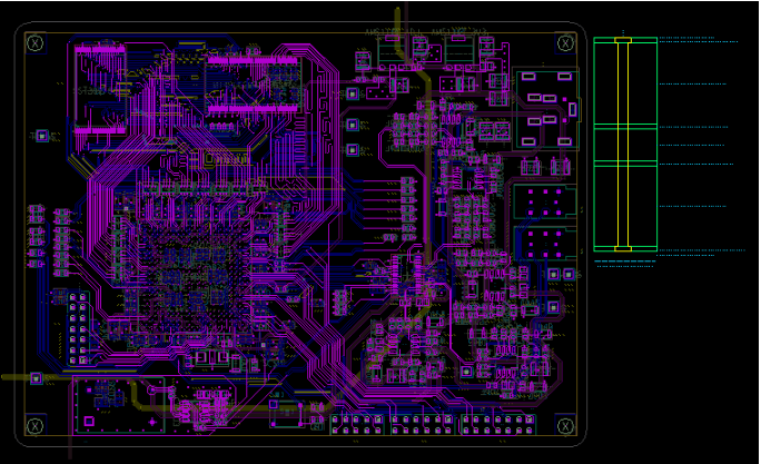


抖音二維碼

Q Q二維碼

微信二維碼
點(diǎn)擊
然后
聯(lián)系
然后
聯(lián)系
電話熱線
13410863085Q Q

微信

- 郵箱