鑫景福致力于滿足“快速服務,零缺陷,輔助研發”PCBA訂購單需求。


行業新聞
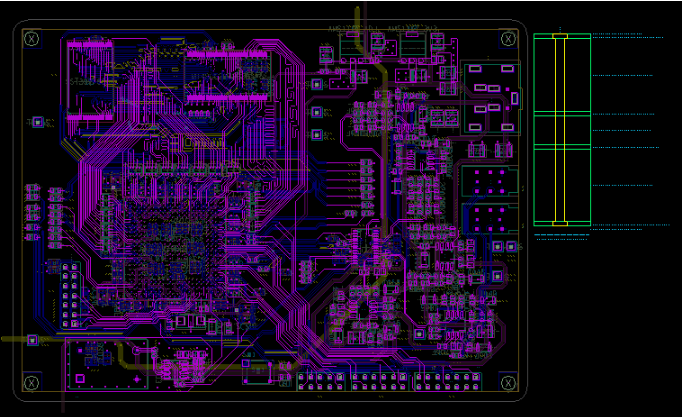
The process of electronIC hardware design includes hardware requirement scheme, schematIC design, PCB proofing, PCB manufacturing, UT and integration testing. In the PCB processing and manufacturing link, in order to ensure the quality of PCB, manufacturers usually use a variety of detection methods for different PCB defects in the production process.
Seven Common Inspection Methods for PCB
PCB board manual visual inspection
It is the most traditional detection method to use magnifier or calibrated microscope and operator's visual inspection to determine whether the circuit board is unqualified and when the correction operation is required. However, due to the increase of output and the reduction of wire spacing and component volume on PCB, this method becoMES more and more infeasible.
Advantages: low budget cost, no test fixture.
Disadvantages: human subjective error, high long-term cost, discontinuous defect detection, difficult data collection, etc.
2. PCB board online test
Find out manufacturing defects and test analog, digital and mixed signal components through electrical performance testing to ensure that they meet specifications. There are several testing methods such as needle bed tester and flying needle tester.
Advantages: low test cost of each board, strong digital and functional test capability, fast and thorough short circuit and open circuit test, programming firmware, high defect coverage and easy programming.
Disadvantages: test fixture is required, programming and debugging time, high cost of making fixture, and difficult to use.
3. PCB board function test
Functional system test is to use special test equipment at the middle and end of the production line to comprehensively test the functional modules of the circuit board to confirm the quality of the circuit board. Function test can be said to be the earliest automatic test principle, which is based on specific boards or specific units and can be completed by various equipment. There are types of final product testing, latest mock ups, and stacked testing. Function test usually does not provide deep data such as pin level and component level diagnosis for process improvement, and requires special equipment and specially designed test flow. Writing function test program is complex, so it is not applicable to most circuit board production lines.
4. Automatic optical inspection
Also known as automatic visual inspection, it is a new method to identify manufacturing defects based on optical principles, using image analysis, computer, automatic control and other technologies to detect and process defects encountered in PCB production. AOI is usually used before and after reflow and before electrical testing to improve the qualification rate of electrical treatment or functional testing. At this time, the cost of correcting defects is far lower than that of conducting the final test, often up to ten times.
5. Automatic X-ray inspection
Take advantage of the different absorptivity of different substances to X-ray, fluoroscopy the parts to be tested, and find defects. It is mainly used to detect defects such as bridging, chip loss, and poor alignment caused by ultra-fine spacing, ultra-High Density Circuit Boards and assembly process. It can also use its tomography technology to detect internal defects of IC chips. It is the only way to test the welding quality of the ball grid array and the shielded solder balls.
Advantages: BGA welding quality and embedded components can be detected without fixture cost.
Disadvantages: slow speed, high failure rate, difficulty in detecting reworked solder joints, high cost and long program development time.
6. Laser detection system
This is the latest development of PCB testing technology. Use laser beam to scan the printed board, collect all measurement data, and compare the actual measurement value with the preset qualified limit value. This technology has been verified on the light plate, and is being considered for assembly plate testing. The speed is enough for mass production lines.
Advantages: Fast output, no fixture and visual non masked access required.
Disadvantages: high initial cost, many maintenance and use problems.
7. Dimension inspection
Use the anime image measuring instrument to measure the hole position, length and width, position and other dimensions. Because PCB is a SMAll, thin and soft type product, contact measurement is easy to deform and cause inaccurate measurement. The anime image measuring instrument has become the best high-precision dimension measuring instrument.
Different detection methods have their own advantages and disadvantages. PCB manufacturers will select appropriate detection methods for different PCB types, complexity, defects and other specific situations to ensure the quality of PCB.


抖音二維碼

Q Q二維碼

微信二維碼
點擊
然后
聯系
然后
聯系
電話熱線
13410863085Q Q

微信

- 郵箱