鑫景福致力于滿足“快速服務,零缺陷,輔助研發”PCBA訂購單需求。


行業新聞
Do you know how PCB is produced? What are the process steps
PCB manufacturers, PCB designers and PCBA manufacturers explain to you: Do you know how PCB is produced? What are the process steps
Although PCB is already well known, we can even say that we deal with it every day.
So, what is it?
How is it produced?
How many manufacturing processes are there?
Let's go into PCB manufacturing factory to explore!
1、 What is PCB
Now that you have come to the PCB manufacturing factory, you must know what PCB is first, right!
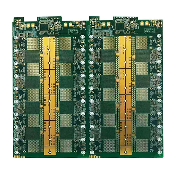
PCB (printed circuit board) is the printed circuit board (PCB for short). It is an important electronIC component, the support of electronIC components, and also the carrier of electrical connection of electronic components.
Today, almost every kind of electronic equipment, ranging from electronic watches and mice to computers and large communication equipment. As long as the electronic components of integrated circuit can be used, PCB will be used.
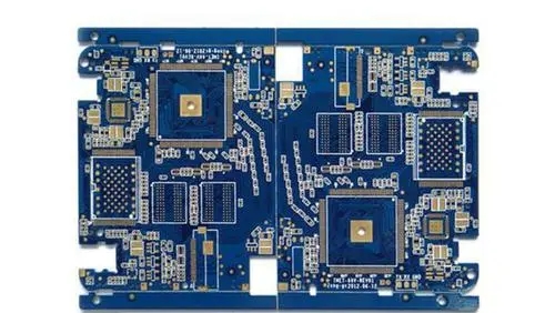
PCB seems very complex, but it is also relatively SIMple.
In fact, many SMAll copper wires are sandwiched between multiple layers of glass fibers. The copper wires can effectively connect each integrated circuit, and then form a new electronic circuit.
01 Receiving and inspection of design board
The engineering department of the factory accepts and checks the design board documents sent by the customer.
The contents to be checked include: whether the design document is appropriate, whether the layer is missing, whether there is a border on the file, whether the drilling file exists, etc.
If the design is flawed, the engineering department will inform the designer to modify it. If there is no design problem, mass production can be carried out according to the design.
02 Print the design into transparencies
Print the checked design documents into transparencies.
The light is projected onto these films, and the photoresist is exposed on the circuit board in a manner similar to the exposure photo. This piece by piece circuit board design is like a movie, lifelike, especially vivid.
03 Cutting and edge grinding of glass fiber
Glass fiber shall be selected and cut and polished.
Select FR-4 glass fiber with copper plating on the top and bottom layers, and then cut the designed size on the cutting machine. Since the edge of glass fiber is too rough, we need to polish its edge.
04 Inner layer fabrication
The top and bottom layers of glass fiber are coated with plastic dry film and hardened under the exposure of ultraviolet ray.
After the dry film on both sides of the glass fiber becoMES hard, the machine is used to press them together, which can effectively prevent the copper from being dissolved by alkaline liquid in the subsequent process.
05 Etching process
The purpose of the entire etching process is to remove the excess copper and photoresist from the copper plate, and complete the prototype of PCB through a series of processes.
Remove the excess copper and photoresist from the pressed glass fiber, complete the etching process through the baptism of alkaline solution, and complete the entire etching process through film stripping, washing, drying and dry plate combination after Z.
06 Automatic Optical Inspection (AOI) and Clip Vacuum (PP)
The purpose of automatic optical inspection is to check the etching of the inner layer and ensure that the etching of the inner layer is normal.
Clip vacuum is to attach the yellow patch similar to epoxy resin to both sides of the board to increase the adhesion.
07 High temperature and high pressure treatment
After 200 ℃ and 27 kg of pressure, the epoxy resin in the melted prepreg sticks the PCB board on both sides to complete the lamination.
08
Drilling technology
Drilling is to use the machine that automatically changes the drill bit to drill out the required empty hole according to the design.
The holes on PCB can be divided into three types: through holes, blind embedded holes and mechanical holes.
In this step of drilling, holes can be drilLED as required to facilitate subsequent operations such as welding of components.
09 Electroplating process
Electroplating requires a complete chEMIcal process.
The place without copper after drilling is plated with copper, so that the PCB can be conductive, and then the copper in the hole is thickened again, because the electroplating is not thick at one time, which requires multiple operations.
10 Solder Mask and Drying
After electroplating, the PCB needs to undergo another optical automatic inspection (AOI), and then the green liquid solder mask can be brushed and dried.
When it comes to the color of PCB, everyone's first reaction must be green, so how did it come from?
The secret is the solder mask.
eleven
Removal, washing and wire mesh of welding mask
After removing the solder mask, we need to solidify the solder mask. After keeping the original state, we need to wash away the unwanted things, remove the pads of the circuit board, and then paste a screen for the customers who need it.
12 Hot air treatment (HASL)
Hot air treatment is to immerse the circuit board into the liquid solder, and then blow off the excess with a hot air sheet after pulling it out.
13 PCB cutting
Since each large PCB has many different small pieces, it also comes from many different customers.
Therefore, we need to cut it.
fourteen
Short circuit and open circuit test
Do you think this is the end?
NO! NO! NO!
Another important link of Z is that we need to test the circuit board for short circuit and open circuit to ensure that each circuit board can be connected normally.
The micro robot arm quickly verifies the electrical connection between the two pads, one after another, which is really a bit incredible.
15 Packaging and Transportation
PCB packaging and transportation are also very particular. After a series of processes such as classification, packaging and labeling are completed, the PCB can be delivered to customers.
Generally, the customer can complete the order 24 hours after placing an order. For domestic orders, it can be delivered within 1-2 days. For international orders, it takes about a week.
3、 Summary
After reading the above sharing, we must also find that the factory production of PCB boards has about 15 processes in total, which is very complicated.
In fact, with the development of science and technology, many jobs that need human resources are gradually being replaced, and the industrial system and technology are also constantly improving and updating. I believe that in the near future, there will be many new innovations in the PCB industry. PCB manufacturers, PCB designers and PCBA manufacturers explain to you: Do you know how PCB is produced? What are the process steps.


抖音二維碼

Q Q二維碼

微信二維碼
點擊
然后
聯系
然后
聯系
電話熱線
13410863085Q Q

微信

- 郵箱