鑫景福致力于滿足“快速服務,零缺陷,輔助研發”PCBA訂購單需求。


行業新聞
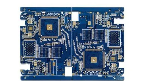
The applICation and significance of printed circuit board
PCB manufacturers, PCB designers and PCBA manufacturers explain the application and significance of PCB
It is the physical support and wiring base of electronic, electrical and mechanical components. The mechanical support of the component is provided by the plate base, which is electrically connected with the bonding pad through the conductive trace. The circuit board consists of a substrate with copper rails, which act as wires connecting components. These components are soldered to the PCB so that they are strongly held. The insulation layer and copper layer on the circuit board contain signal traces of power supply and grounding.
Traditionally, components are instalLED in the holes in the upper layer of Z, so that they can pass through all layers. These were later referred to as through-hole assemblies. With the near universal use of surface mount components, it is generally found that components are mounted on the top and bottom layers of two printed circuit boards.
Classification of polychlorinated biphenyls
printed circuit boards can be classified according to manufacturing process and substrate materials, such as:
Based on the number of layers
Type of substrate, i.e. organic or inorganic
Physical structure or design, i.e. rigid, flexible or sEMI-rigid
Conductor pattern design based on application
Inorganic alkali, discrete wiring, additive, multi wire and wire package are completely eliminated with the overall progress of technology.
Before entering the details of PCB classification, let's first understand PCB terminology.
Structure and terminology of polychlorinated biphenyls
It is a complex process to transform application design into printed circuit board. It is another complicated process to maintain the standards of through-hole, base plate and protective pad, grounding and trace while designing PCB. The structure of the printed circuit board shall comply with the designer's recommendations, such as the size of the printed circuit board, possible track width, gap between tracks, etc.
Any manufacturing work order shall provide guidelines on the size requirements, pass through requirements, fill requirements, and original dimensions of the backing plates so that these specifications can be considered. For example, if a 150 mil rail is required, a 100 mil rail and a 55 mil rail can be placed side by side with an overlap of 5 mils to obtain a 150 mil rail.
Traces and spacing between them
A trace is a copper wire that electrically connects two or more points on a PCB. Carry a SMAll amount of current. The process of placing traces on a PCB can be electroplating or etching on the substrate surface to create the desired pattern. Etching methods are common in the electronic industry.
The thickness of copper on the PCB is measured in ounces (ounces) per square foot. In general, 1 ounce and 1 ounce copper are commonly used by Z. Thicker copper up to 6 ounces is used for high current and reliability designs.
The design of trace width, trace thickness, trace spacing, signal trace layout, power and ground traces and wiring in Printed Circuit Board (PCB) layout are based on design calculation and design rules and standards. So why is there such a calculation?
Track width design is based on separate current carrying capacity and temperature resistance. The resistance to the current generates heat, which is dissipated by the trace, depending on the surface area, air flow and solder mask thickness. Wider traces generate less heat and are easy to lose.
The spacing between channels, in other words, electrical clearance is very important. It is recommended to leave as much space as possible. The track spacing and trace width depend on the current flowing through the track and the temperature rise of the track.
IPC has a set of standards on clearance and spacing according to environmental conditions (excluding voltage). Generally, the signal tracking maintains the width, while the power tracking and ground tracking have a large width, and their spacing can be 40 μ m-60 μ M. The edge spacing is very important for the debonding process (125 mils recommended).
Protective pad
The pad is a small area of copper sheet used to connect the pins of parts. Backing means that the predetermined shape is removed from the copper.
In general, reverse pads are used around through holes to isolate them from power planes that do not need to be connected.
Grounding
A bonding pad is required to weld components on the top or bottom layer of a printed circuit board, which is called grounding.
The size, shape and size of the mat depend on:
1. Type of component package being used.
2. Manufacturing process for assembling cardboard.
According to IPC standards and design rules, SMT gasket conductor length diameter ratio, THT hole conductor length diameter ratio, THT ring, package size and pitch are defined. SometiMES manufacturers define their choices. For example, the size of the BGA pad depends on the surface finish. For HASL surface finish, BGA gasket size is 12 mil (1 mil=0.001 inch) diameter, for other surface finishes, 10 mil diameter will remain the same.
Through-hole
Through holes are metal sheets connecting different layers of PCB. It connects one side of the plate to the other through holes in the plate. PTH (electroplated through-hole), micro through-hole and through-hole pad all belong to through-hole category.
Through holes transmit signals or power between layers through PTH. The size of the pass depends on the trace width. Some micro through-holes used between layers are called buried through-holes, and those used between the outer layer and the inner layer are called blind through-holes, which are used when high-density internal connections are required.
Single sided polychlorinated biphenyls
Single sided PCB only contains one layer of conductive material, and Z is suitable for low density design. The components are arranged on one side and the circuits are arranged on the other side. In circuit design, the circuit board is limited, because the conduction only occurs on one side, and cross (conduction) is not allowed. Each line must have its own path.
Single sided printed circuit board is the basic starting point of printed circuit technology Z. It is indeed the starting point of an invention, because it plays an important role in the industrial production of low-cost, mass production of SIMple circuits.
Monolayer PCBs have relatively broad applications ranging from power supplies, relays, sensors and LED calculators, printers, coffee machines and electronic toys. However, single-sided printed circuit boards also have some performance limitations.
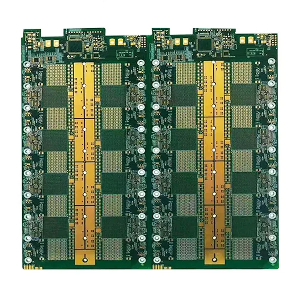
Double sided polychlorinated biphenyls
It is a common and widely used board class in Z. Double layer polychlorinated biphenyls have two conductive layers and traces, which are placed on both sides of a substrate, so they are components. Due to the complexity and increased density of components, many PCBs need to use two sides. PCB manufacturers, PCB designers and PCBA manufacturers will explain the application and significance of PCB to you.


抖音二維碼

Q Q二維碼

微信二維碼
點擊
然后
聯系
然后
聯系
電話熱線
13410863085Q Q

微信

- 郵箱