鑫景福致力于滿足“快速服務,零缺陷,輔助研發”PCBA訂購單需求。


行業新聞
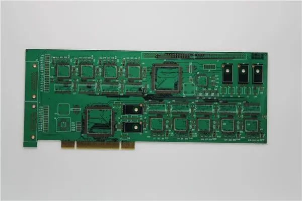
The board manufacturer introduces the definition of HDI board
Circuit board manufacturer, circuit board design and PCBA processing manufacturer explain to you: circuit board manufacturer introduces the definition of HDI circuit board
The appearance of HDI printed circuit board fully meets the requirements of miniaturization, lightweight and thinness of electronIC products, which is a major change in the manufacturing technology of conventional multilayer printed circuit board. The manufacturing technology of HDI printed circuit board not only includes the manufacturing of buried holes and blind holes, such as laser drilling, photoinduced drilling, plaSMA etching and other hole forming technologies and their electrical interconnection technologies, but also has emerged a batch of new substrate materials (such as resin coated copper foil) and coating materials. At the same time, there are new developments in product processing equipment, positioning systems, product inspection and other aspects.
HDI printed boards are calLED build up multilayer (BUM) in Japan. There are many manufacturing methods for it, such as SLC (surface laser circuit) technology using photo induced pore forming method; CLLAVIS (CMK mining multi laser via hole system) technology with resin coated copper foil and laser drilling is adopted; ALIVH (any layer inner via hole) technology and Bz it (built bump interconnection technology) technology using conductive paste to realize electrical interconnection.

Definition of HDI PCB
American PCB manufacturer in 1994 In April, a cooperative society ITRI (Interconnection Technology Research Institute) was formed
In September of the same year, we carried out research on the production of high-density circuit boards, specifically called the October Project
Motorola's test samples MTV1 and MRTV2.2 (1996.6) were used successively
Make micro blind holes by non machine drilling, such as laser ablation, photosensitive photoforming, photo Via, plasma Etching and alkali etching, and conduct quality and reliability evaluation.
On July 15, 1997, the report of October Project Phase 1 Round 2, which was evaluated by Microvia, was published
Expand the new era of "high-density interconnection HDI".
Definition of HDI
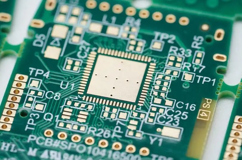
For non mechanical drilling, the obtained hole diameter is less than 0.15 mm (6 mil) (most of them are blind holes), and the ring diameter of the annular ring or pad or land is less than 0.25 mm (10 mil), which is specifically called Microvia micro pilot hole or micro hole.
A PCB with micropores, a connection density of more than 130 points per square inch, and a wiring density (50 mil for a channel) of more than 117 inches per square inch is called HDI PCB, with a line width/spacing of 3 mil/3 mil or thinner and narrower.
In fact, this High Density Interconnection is not very different from the earlier popular Build up Multilayer. The main difference between them and traditional PCBs is the hole forming method.
After several years of trials, laser drilling has become the mainstream of the four non mechanical drilling methods. Carbon dioxide lasers are produced in the micro blind holes of mobile phone boards above 5mil, while YAG lasers are used in the field of packaging carrier boards below 3mil.
HDI's MARKet Products
According to different product characteristics, HDI micro blind hole laminate can be widely used for:
1. For mobile phones and laptops, the former mostly aim to be light, thin, short and functional, while the latter is to enhance the quality of key signal lines, so there are few holes.
2. High order computer and network communication, as well as surrounding large high layer boards (High Layer Count above 14 layers), are targeted at "Signal Integrity" and high functional boards controlled by strict characteristic impedance, with a small number of holes.
3. Packaging Substrate covers various precision carrier plates (also known as interposer or Module Board) of Wine Board and Flip chip. The L/S reaches 2mil/2mil, and the aperture is only 1-2mil, and the hole spacing is also less than 5mil. HDI product example ALIVH (Any Layer Interstitial Via Hole)
The finished double-sided inner layer board, the film with copper paste and the outer copper skin are pressed together to form a complex multilayer board. The yield is better than the successive layer adding method because of the one-time completion.
ALIVH EXISTING
① Standard ALVIH is used in mobile phone boards, accounting for 60%, and is more adopted by Nokia and Ericaon
② ALIVH-B can be used for larger precision motherboards ③ ALIVH-FB can be used for various extremely precise packaging carriers (Substrates)
PCB manufacturers, PCB designers and PCBA processors will explain to you the definition of HDI PCB.


抖音二維碼

Q Q二維碼

微信二維碼
點擊
然后
聯系
然后
聯系
電話熱線
13410863085Q Q

微信

- 郵箱