鑫景福致力于滿足“快速服務,零缺陷,輔助研發”PCBA訂購單需求。


行業新聞
SMT automatIC X-ray detector and its development prOSPect
About PCBA factory automatic X-ray detector
X-ray has a strong penetrability and is the first instrument used in various testing occasions. X-ray fluoroscopy image can show the density distribution of solder joint thickness, shape and quality. These quotas can fully reflect the welding quality of solder joints, including open circuit, short circuit, holes, holes, internal bubbles and tin deficiency, and can be used for quantitative analysis. The X-ray is generated by the micro focus X-ray EMIssion tube, passing through the window in the tube and projecting onto the sample. The X-ray absorptivity of the sample depends on the composition and proportion of the data contained in the sample. The X-ray passing through the sample bombards the iodine coating on the X-ray sensitive plate and excites photons. The CAMera detects these photons to generate signals, then processes and amplifies them, and the computer further analyzes and observes them. Different sample data have different opacity coefficients for X-ray, and the processed gray image can show the difference between the density of the detected object and the thickness of the data.

Definition and function of SMT process file
At present, there are two kinds of X-ray detectors that are used frequently, one is direct X-ray detector, the other is 3D X-ray layered scanning detector. The former is cheap, but it can only provide two-dimensional image information, and it is difficult to analyze the mask part. The latter can detect inherent defects of solder joint, hidden solder joint defects of BGA and other planar array devices, and related inherent defects of components themselves. 3D X-ray layered scanning detector This detection technology uses the scanning beam X-ray layered photography technology to obtain 3D image information and eliminate shadows. It is combined with computer image processing technology to detect the solder joints in the inner layer of PCB and shape memory alloy with high resolution, especially suitable for detecting hidden solder joints under BGA, CSP and other packaging devices. Through the 3D image of the solder joint, the 3D size of the solder joint, the amount of solder and the wetting state of solder can be measured, and the solder joint defects can be accurately and objectively determined. The quality of metallized through-hole of printed circuit board can also be nondestructive tested. At present, the relatively advanced 3D X-ray layered scanning technology still has some limitations in practical application, such as the detection of internal microcracks, which needs to be further improved.
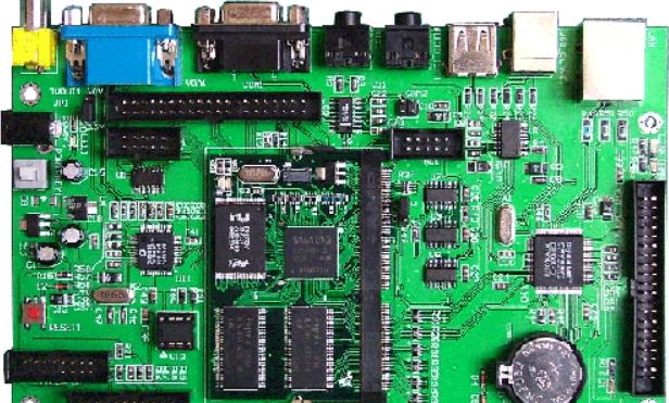
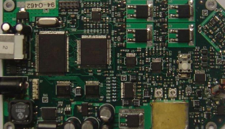
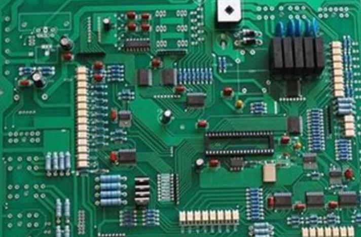
circuit board
Problems and future development trend of SMT patch AI
Although AOI is more efficient than artificial vision detection, after all, its results are obtained through image acquisition and analysis processing, and the software technology related to image analysis and processing has not reached the level of human brain. This, in actual use, inevitably there will be some special circumstances, such as miscalculation and omission of AOI. In this regard, pattern recognition and intelligence will become the development direction of AOI technology.
1) Graphic recognition method has become the mainstream of application
Due to the rapid development of the main detection objects (such as SMD components, PCB circuits, solder paste printing graphics, etc.) used by AOI technology in SMT, it is difficult to fully keep up with the corresponding design rules and standards. Recall that DRC method based on design rules is difficult to apply, and the rapid development of computer technology has solved the problem of high-speed graphics processing, making the graphics recognition method more practical. At present, all kinds of pattern recognition AOI technologies are more and more widely used in SMT.
2) AOI technology is developing towards intelligence
With the miniaturization, high density, rapid assembly and diversification of Surface Mount Technology, the detection information is large and complex. Whether in terms of real-time detection echo or accuracy of analysis and diagnosis, it depends on manual work. It is almost impossible to analyze and diagnose the quality information obtained by artificial intelligence. The intelligent artificial intelligence technology that replaces manual and automatic analysis and diagnosis has become an inevitable development. The schematic diagram of the intelligent AOI system uses solder joint shape recognition and expert system analysis. It is based on the theory and method of solder joint shape SIMilar to automatic visual inspection, that is, measuring the shape of solder joint on the line using optical system and image processing measures. The computer will compare the actual shape of the solder joints obtained with the reasonable shape of the system inventory, quickly identify the faulty solder joints that exceed the allowable shape range, and use SMArt technology to automatically analyze and evaluate their fault types and causes, forming real-time control information for process parameter optimization and adjustment, real-time echo control for solder joint quality, and recording and statistical processing of analysis and evaluation information.


抖音二維碼

Q Q二維碼

微信二維碼
點擊
然后
聯系
然后
聯系
電話熱線
13410863085Q Q

微信

- 郵箱