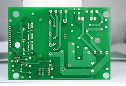
What are the precautions and operating skills in PCB design
For experienced engineers, the PCB design is very SIMple, and all kinds of precautions and operating skills are readily available and very skilLED It is diffICult for new engineers to master the skills of circuit board design After all, their proficiency is not enough, and there will be problems in the design Therefore, it is necessary to understand circuit board design So, what are the PCB design skills?
circuit board
What are the precautions and operating skills in circuit board design
Skill 1: The definition of processing level should be clear
When there is unclear place in the file, the engineer must be asked to check it, so as to reduce the chance of making plate mistakes. Not only that, but also pay attention to special instructions when designing single-sided circuit boards. If there is no special instructions, such as the front and back, the designed circuit board may not be soldered. Please note this.

Tip 2: The copper foil should not be too close to the outer frame
According to the experience of the engineer, the distance between the large area copper foil and the outer frame should be kept at least 0.2mm, so special attention should be paid during operation. If the distance is less than 0.2mm, there is a risk that the solder resist will fall off.
Tip 3: Pads cannot be drawn with fill
Many beginners will ignore this technology, because it is possible to use filler blocks to draw pads in circuit Board Design, which can pass DRC inspection, but cannot be used during processing, because such pads cannot directly generate welding masks. When a solder mask is used, the area will be covered by the solder mask, making it difficult to weld components.
Tip 4: Power grounding cannot coexist with pads and wires
When some engineers are designing circuit boards, the electrical ground plane looks like a flower pad and a connection. This is wrong. Because the ground plane is different from the actual PCB image, they are opposite. All connections are obstacle lines, and no gap can be left. Otherwise, it is easy to cause power short circuit.
Tip 5: The mat cannot be too short
If the gasket of the surface mount assembly is too short, the test pin can easily be misaligned. Because the mat is too dense, the distance between the feet is very SMAll, and the mat is also very thin. When installing the test pin, it must be staggered up and down, otherwise this will happen.
Tip 6: Pads cannot overlap
Overlapping gaskets can easily lead to scrapping during drilling Therefore, the gaskets must not overlap These are the six skills of circuit board design that only skilled people can master The technical content of these technologies is not very high, but it greatly affects the results of circuit board design Therefore, in the process of PCB design, we must pay attention to these points to achieve perfection
The above is the explanation given by the editor of pcb circuit board company. If you want to know more about PCBA, you can go to our company's home page to learn about it. In addition, our company also sells various circuit boards,
High frequency circuit board and SMT chip are waiting for your presence again.
然后
聯(lián)系
電話(huà)熱線(xiàn)
13410863085Q Q

微信

- 郵箱


