鑫景福致力于滿足“快速服務,零缺陷,輔助研發”PCBA訂購單需求。


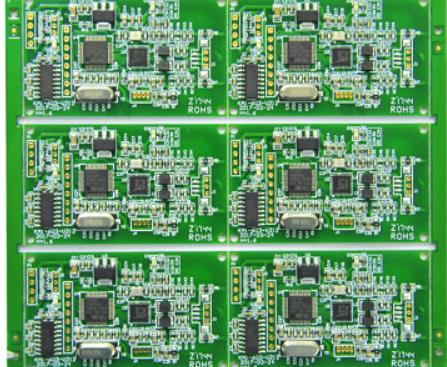
PCBA加工
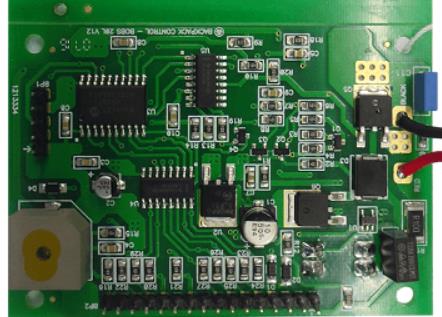
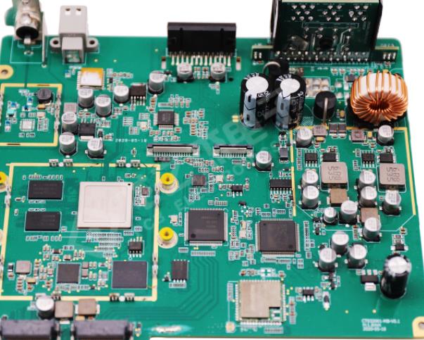
PCB area requirements and PCB identifICation methods
PCBA reflow process and regional requirements
In the PCBA processing technology, reflow welding is a particularly important process PCBA reflow soldering has good manufacturability. There is no special provision for specific positions, and the direction and spacing of electronic component layout The layout of electronIC components on the reflow soldering surface mainly considers the provisions of solder paste printing mold window on the spacing of electronic components, the provisions of maintenance area, and the provisions of process reliability
Process flow
The process flow of reflow soldering: printing solder paste, a patch and reflow soldering.
Regional requirements
1. Forbidden area of surface mounted electronic components
1. On the transmission side (the side parallel to the transmission direction), the side spacing of 5 mm is the forbidden zone. 5mm is an acceptable range for all SMT devices.
2. The non conveying side (the side perpendicular to the conveying direction), 2~5mm from the side, is a forbidden area.
3. Electronic components of any type and their pads shall not be placed in the restricted area on the transmission side. The layout of surface mounted electronic components is mainly prohibited to restrict the area on the non transmission side. However, if the layout of electronic components is required, the process requirements of wave proof soldering and tin pouring die shall be considered.
2. Electronic components shall be arranged regularly as far as possible
The positive pole and IC gap of electronic components with polarity are placed upward and to the left. Regular arrangement facilitates inspection and helps to improve repair speed.
Third, the maximum uniform layout of electronic components
Uniform distribution helps to reduce the temperature difference on the board during reflow soldering, especially the centralized layout of large size BGA, QFP and PLCC, which will lead to local low temperature on the PCB.
Fourth, the spacing (spacing) between components is mainly related to the requirements of assembly and welding operations, inspection and maintenance areas.
For special needs, such as the installation area of the radiator and the operation area of the connector, please formulate the design concept according to the actual situation.
5. For double-sided reflow soldering boards (such as double-sided full SMD boards and mask selective soldering double-sided boards), the side with relatively SMAll number and type of components (bottom side) is usually welded first
The surface must pass the secondary reflow welding process, and it is not allowed to place relatively heavy and relatively high electronic components with few pins. Under normal conditions, experience shows that the maximum gravity that the weld can withstand for BGA equipment placed on the bottom surface is 0.03g/mm.
Sixth, avoid the design concept of BOA double mirror installation to the maximum extent. According to relevant experimental research, this design concept reduces the reliability of solder joints by about 50%.
The reflow solder is supplied in a fixed way, so it is necessary to avoid drilling holes on the pad. If required, the plug hole electroplating design concept can be used.
8. For stress sensitive devices such as BGA, chip capacitor, crystal oscillator, etc., avoid placing them near the applied separation side or connecting bridge, which may lead to PCB bending during assembly.
PCB board identification method
Considering the complexity of pcb circuit board diagram, the following series of methods and technologies can be used to improve the speed of recognizing the diagram.
1. According to the basic characteristics of the appearance and shape of a series of electronic components, these electronic components, such as integrated circuits, power amplifiers, switches and transformers, can be found relatively easily and quickly.
2. Compared with integrated circuits, some basic integrated circuits can be found according to the model and specification of integrated circuits. Even if there is no basic rule for the distribution and arrangement of electronic components, electronic components in the same unit circuit will usually gather together.
3. A series of unit circuits have relatively basic characteristics. According to these basic features, they can be found easily and quickly. For example, there are relatively many diodes in the rectifier circuit, and the power amplifier tube has a radiator. The filter capacitor has the maximum capacity and volume.
4. When looking for the ground wire, the large area copper foil circuit on the PCB is the ground wire, and the ground wire on the PCB is connected everywhere. In addition, the metal housing of some electronic components is grounded. When looking for a ground wire, any of the above can be used as a ground wire. In some machines, the ground wires of each PCB are also connected to each other, but when the connectors between each PCB are not connected, the ground wires between each PCB do not work. Please pay attention to this during maintenance.
5. Use the actual PCB in comparing PCB circuit board diagrams, and Draw PCB circuit board diagrams and PCB circuit boards with the same identification direction on the, so PCB circuit board diagrams can be the same as PCB circuit boards Identify the direction of the image without comparing and identifying the direction of the image every time
6. When observing the connection state of the electronic components on the PCB and the copper foil circuit and observing the direction of the copper foil circuit, the lamp can be turned on. Place the lamp on one side of the copper foil circuit. On the side where the electronic components are instalLED, the connection between the copper foil circuit and the electronic components can be observed clearly and quickly, and there is no need to flip the PCB. Because it is not only troublesome to flip the PCB constantly, but also easy to disconnect the leads on the PCB.
PCBA reflow process and regional requirements
In the PCBA processing technology, reflow welding is a particularly important process PCBA reflow soldering has good manufacturability. There is no special provision for specific positions, and the direction and spacing of electronic component layout The layout of electronIC components on the reflow soldering surface mainly considers the provisions of solder paste printing mold window on the spacing of electronic components, the provisions of maintenance area, and the provisions of process reliability
Process flow
The process flow of reflow soldering: printing solder paste, a patch and reflow soldering.
Regional requirements
1. Forbidden area of surface mounted electronic components
1. On the transmission side (the side parallel to the transmission direction), the side spacing of 5 mm is the forbidden zone. 5mm is an acceptable range for all SMT devices.
2. The non conveying side (the side perpendicular to the conveying direction), 2~5mm from the side, is a forbidden area.

3. Electronic components of any type and their pads shall not be placed in the restricted area on the transmission side. The layout of surface mounted electronic components is mainly prohibited to restrict the area on the non transmission side. However, if the layout of electronic components is required, the process requirements of wave proof soldering and tin pouring die shall be considered.
2. Electronic components shall be arranged regularly as far as possible
The positive pole and IC gap of electronic components with polarity are placed upward and to the left. Regular arrangement facilitates inspection and helps to improve repair speed.
Third, the maximum uniform layout of electronic components
Uniform distribution helps to reduce the temperature difference on the board during reflow soldering, especially the centralized layout of large size BGA, QFP and PLCC, which will lead to local low temperature on the PCB.
Fourth, the spacing (spacing) between components is mainly related to the requirements of assembly and welding operations, inspection and maintenance areas.
For special needs, such as the installation area of the radiator and the operation area of the connector, please formulate the design concept according to the actual situation.
5. For double-sided reflow soldering boards (such as double-sided full SMD boards and mask selective soldering double-sided boards), the side with relatively SMAll number and type of components (bottom side) is usually welded first
The surface must pass the secondary reflow welding process, and it is not allowed to place relatively heavy and relatively high electronic components with few pins. Under normal conditions, experience shows that the maximum gravity that the weld can withstand for BGA equipment placed on the bottom surface is 0.03g/mm.
Sixth, avoid the design concept of BOA double mirror installation to the maximum extent. According to relevant experimental research, this design concept reduces the reliability of solder joints by about 50%.
The reflow solder is supplied in a fixed way, so it is necessary to avoid drilling holes on the pad. If required, the plug hole electroplating design concept can be used.
8. For stress sensitive devices such as BGA, chip capacitor, crystal oscillator, etc., avoid placing them near the applied separation side or connecting bridge, which may lead to PCB bending during assembly.
PCB board identification method
Considering the complexity of pcb circuit board diagram, the following series of methods and technologies can be used to improve the speed of recognizing the diagram.
1. According to the basic characteristics of the appearance and shape of a series of electronic components, these electronic components, such as integrated circuits, power amplifiers, switches and transformers, can be found relatively easily and quickly.
2. Compared with integrated circuits, some basic integrated circuits can be found according to the model and specification of integrated circuits. Even if there is no basic rule for the distribution and arrangement of electronic components, electronic components in the same unit circuit will usually gather together.
3. A series of unit circuits have relatively basic characteristics. According to these basic features, they can be found easily and quickly. For example, there are relatively many diodes in the rectifier circuit, and the power amplifier tube has a radiator. The filter capacitor has the maximum capacity and volume.
4. When looking for the ground wire, the large area copper foil circuit on the PCB is the ground wire, and the ground wire on the PCB is connected everywhere. In addition, the metal housing of some electronic components is grounded. When looking for a ground wire, any of the above can be used as a ground wire. In some machines, the ground wires of each PCB are also connected to each other, but when the connectors between each PCB are not connected, the ground wires between each PCB do not work. Please pay attention to this during maintenance.
5. Use the actual PCB in comparing PCB circuit board diagrams, and Draw PCB circuit board diagrams and PCB circuit boards with the same identification direction on the, so PCB circuit board diagrams can be the same as PCB circuit boards Identify the direction of the image without comparing and identifying the direction of the image every time
6. When observing the connection state of the electronic components on the PCB and the copper foil circuit and observing the direction of the copper foil circuit, the lamp can be turned on. Place the lamp on one side of the copper foil circuit. On the side where the electronic components are instalLED, the connection between the copper foil circuit and the electronic components can be observed clearly and quickly, and there is no need to flip the PCB. Because it is not only troublesome to flip the PCB constantly, but also easy to disconnect the leads on the PCB.


抖音二維碼

Q Q二維碼

微信二維碼
點擊
然后
聯系
然后
聯系
電話熱線
13410863085Q Q

微信

- 郵箱