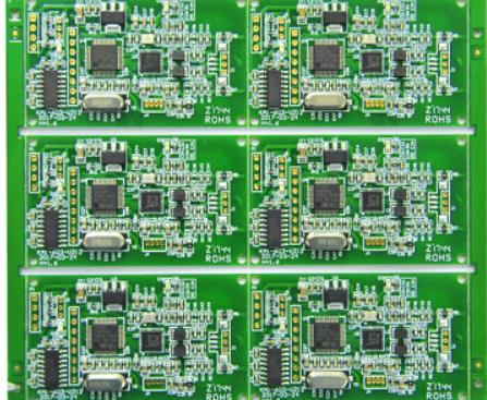
鑫景福致力于滿足“快速服務,零缺陷,輔助研發”PCBA訂購單需求。


PCBA加工
Precautions for PCB testing and PCB SMT wafer processing
PCB board test
The production process of PCB chip processing is very complex, including many important processes such as PCB manufacturing process, component procurement and inspection, SMT chip assembly, DIP parts and PCB test. Among them, PCB testing is the most critICal quality control link in the whole PCB processing process, which affects the final use efficiency of products. What is the test form of PCB?
PCB test mainly includes five forms: ICT test, FCT test, aging test, fatigue test and harsh environment test.
1. ICT test mainly includes circuit on-off, voltage and current value, fluctuation curve, amplitude, noise, etc.
2. FCT test requires IC program startup, analog test of the basic functions of the entire PCB, find out the problems in hardware and software, and provide necessary wafer processing production fixtures and test racks.
3. The fatigue test is mainly to sample PCB circuit boards, conduct high-frequency and long-term operation of basic functions, observe whether there is a fault, and judge the probability of failure in the test, so as to echo the working efficiency of PCB circuit boards in electronic products.
5. The aging test is mainly to power on PCB and electronic products for a long time, maintain their work, and observe whether there is any fault. After aging test, electronic products can be sold in batches.
The production process of PCB is complex. In the process of production and processing, various problems may occur due to improper equipment or operation, and the products produced cannot be guaranteed to be qualified. In this case, PCB needs to be tested to ensure that each product will not have product quality problems.
Precautions SMT chip process inertial navigation and guidance belongs to PCB
The main purpose of SMT chip processing is to accurately install surface mounted electronIC components on the fixed position of PCB What SMT chip processing should we pay attention to when performing? Next, I will introduce the following aspects in detail
1. No food or drink is allowed in the working area of pcb circuit board, no smoking is allowed, no articles irrelevant to work are allowed to be placed, and the workbench should be kept clean and tidy.
2. Regularly check the EOS/ESD workbench to ensure its normal operation (anti-static). Various risks of EOS/ESD components may be caused by incorrect grounding methods or oxides in grounding connection components. This shall provide special protection for the "third wire" grounding terminal connector.
3. Do not stack PCB boards, otherwise physical damage may occur. There shall be various special supports on the assembly working surface, which shall be placed according to the type.
4. During the SMT chip processing of PCB, do not pick up the welding surface with bare hands or fingers, because the grease secreted by human hands will reduce the solderability, and welding defects are likely to occur.
5. Minimize the operation steps of PCB and electronic components to prevent risks. In assembly areas where gloves must be used, soiLED gloves can cause contamination. In this case, gloves must be replaced frequently when necessary.
Do not use skin protection oil on your hands or various silicone based detergents, as they may cause problems with the solderability and adhesion of conformal coatings. A specially formulated cleaner for the soldering surface of PCB.
7. In the SMT chip processing of PCB circuit board, these operating rules should be strictly followed. Correct operation can ensure the final use quality of the product, reduce the damage of electronic components, and reduce costs.
8 Electronic components and PCB boards sensitive to EOS/ESD must be MARKed with appropriate EOS/ESD marks to prevent confusion with other electronic components In addition, in order to prevent ESD and EOS from endangering sensitive electronic components, all operations, assembly and testing must be completed on a workbench capable of controlling static electricity
PCB board test
The production process of PCB chip processing is very complex, including many important processes such as PCB manufacturing process, component procurement and inspection, SMT chip assembly, DIP parts and PCB test. Among them, PCB testing is the most critICal quality control link in the whole PCB processing process, which affects the final use efficiency of products. What is the test form of PCB?
PCB test mainly includes five forms: ICT test, FCT test, aging test, fatigue test and harsh environment test.
1. ICT test mainly includes circuit on-off, voltage and current value, fluctuation curve, amplitude, noise, etc.
2. FCT test requires IC program startup, analog test of the basic functions of the entire PCB, find out the problems in hardware and software, and provide necessary wafer processing production fixtures and test racks.
3. The fatigue test is mainly to sample PCB circuit boards, conduct high-frequency and long-term operation of basic functions, observe whether there is a fault, and judge the probability of failure in the test, so as to echo the working efficiency of PCB circuit boards in electronic products.

5. The aging test is mainly to power on PCB and electronic products for a long time, maintain their work, and observe whether there is any fault. After aging test, electronic products can be sold in batches.
The production process of PCB is complex. In the process of production and processing, various problems may occur due to improper equipment or operation, and the products produced cannot be guaranteed to be qualified. In this case, PCB needs to be tested to ensure that each product will not have product quality problems.
Precautions SMT chip process inertial navigation and guidance belongs to PCB
The main purpose of SMT chip processing is to accurately install surface mounted electronIC components on the fixed position of PCB What SMT chip processing should we pay attention to when performing? Next, I will introduce the following aspects in detail
1. No food or drink is allowed in the working area of pcb circuit board, no smoking is allowed, no articles irrelevant to work are allowed to be placed, and the workbench should be kept clean and tidy.
2. Regularly check the EOS/ESD workbench to ensure its normal operation (anti-static). Various risks of EOS/ESD components may be caused by incorrect grounding methods or oxides in grounding connection components. This shall provide special protection for the "third wire" grounding terminal connector.
3. Do not stack PCB boards, otherwise physical damage may occur. There shall be various special supports on the assembly working surface, which shall be placed according to the type.
4. During the SMT chip processing of PCB, do not pick up the welding surface with bare hands or fingers, because the grease secreted by human hands will reduce the solderability, and welding defects are likely to occur.
5. Minimize the operation steps of PCB and electronic components to prevent risks. In assembly areas where gloves must be used, soiLED gloves can cause contamination. In this case, gloves must be replaced frequently when necessary.
Do not use skin protection oil on your hands or various silicone based detergents, as they may cause problems with the solderability and adhesion of conformal coatings. A specially formulated cleaner for the soldering surface of PCB.
7. In the SMT chip processing of PCB circuit board, these operating rules should be strictly followed. Correct operation can ensure the final use quality of the product, reduce the damage of electronic components, and reduce costs.
8 Electronic components and PCB boards sensitive to EOS/ESD must be MARKed with appropriate EOS/ESD marks to prevent confusion with other electronic components In addition, in order to prevent ESD and EOS from endangering sensitive electronic components, all operations, assembly and testing must be completed on a workbench capable of controlling static electricity


抖音二維碼

Q Q二維碼

微信二維碼
點擊
然后
聯系
然后
聯系
電話熱線
13410863085Q Q

微信

- 郵箱