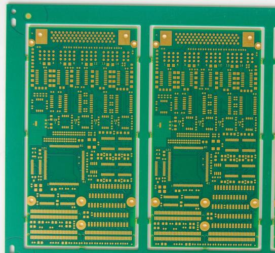
鑫景福致力于滿足“快速服務,零缺陷,輔助研發”PCBA訂購單需求。


PCBA方案設計
How to Prevent Noise in PCB Design
How to prevent noise in PCB design? Can you give a brief description of the coupling effect?
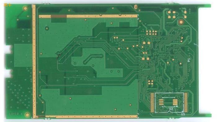
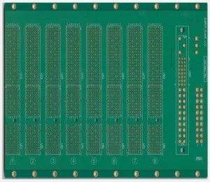
The design of printed circuit board is based on the circuit schematIC diagram to realize the functions required by the circuit designer. The design of printed circuit board mainly refers to layout design, which needs to consider the layout of external connections. The optimal layout of internal electronIC components, the optimal layout of metal wiring and through-hole, electromagnetic protection, heat dissipation and other factors. Excellent layout design can save production costs and achieve good circuit performance and heat dissipation. SIMple layout design can be realized by hand, while complex layout design needs to be realized by computer aided design (CAD).
There are many ways for electrical products to prevent noise. For digital signals, it is not that noise is not allowed to be generated. Instead, the circuit structure should be designed to generate the allowable level of noise, that is, the signal can be identified.
As for the coaxial cable used by cable TV, it uses single core copper wire for signal transmission, but it is an example of noise prevention by covering the metal net around it for noise shielding. This idea appears in many PCBA processing designs, for example, embedding signal lines into the circuit board to protect the transmission signal with a larger copper surface to avoid noise interference. The special design of some circuit boards also has similar functions. For example, for the circuit board surface lines, some products are coated with a layer of conductive paste on the solder stop paint to shield the noise. These are typical examples of noise prevention. Noise exists everywhere, but it must be less than the allowable range of product design, which is the key point.
Coupling effect refers to the influence of electromagnetic induction interaction between two parallel lines, which will change the transmitted signal. When the electric field changes, according to "Lenz's Law", the line environment will have a magnetic field to prevent the change of the electric field, and this magnetic field will certainly have an electrical impact on another adjacent line. This interaction is calLED "coupling effect". Detailed descriptions of detailed principles can be found in books on electrical design and electrical and electronic principles. There are also many such books available for reference in all China science and technology books.
The quality of signal in Fourier transmission line (including signal line, dielectric layer and ground plane) is mainly composed of square wave front working voltage and rise time. When the quality of the transmission line is poor, the signal will rebound, scatter and leak, forming the signal antenna (dB per cm) effect. Therefore, the thickness and width of the signal line, the thickness and Dk of the dielectric layer (water cannot be absorbed, because the Dk of water is 75), and the integrity of the grounding copper surface should be mastered. The above is for your reference.


抖音二維碼

Q Q二維碼

微信二維碼
點擊
然后
聯系
然后
聯系
電話熱線
13410863085Q Q

微信

- 郵箱