鑫景福致力于滿足“快速服務,零缺陷,輔助研發(fā)”PCBA訂購單需求。


PCBA方案設計
Distance between PCB design parts and board edge
How much distance must be left between parts and board edge during PCB design
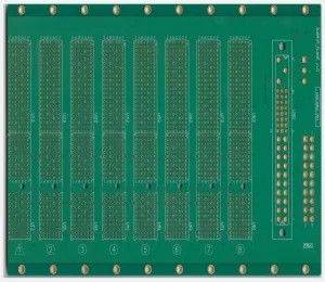
The design of printed circuit board is based on the circuit schematIC diagram to realize the functions required by the circuit designer. The design of printed circuit board mainly refers to layout design, which needs to consider the layout of external connections. The optimal layout of internal electronIC components, the optimal layout of metal wiring and through-hole, electromagnetic protection, heat dissipation and other factors. Excellent layout design can save production costs and achieve good circuit performance and heat dissipation. SIMple layout design can be realized by hand, while complex layout design needs to be realized by computer aided design (CAD).
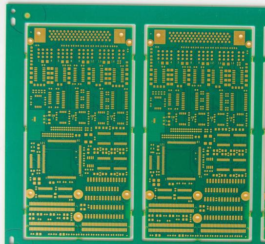
During PCB design, how far must be left between the part and the board edge to avoid affecting the electrical property? (If the material is FR4, there are SMT parts on both sides, connecting plate design, and routing and V-CUT processing between plates) If the width of the angular ring of the force amplifier can control the tolerance of the finished aperture more effectively?
This problem has a lot to do with SMT processing equipment. For most equipment, 0.150 inch of plate edge shall be reserved at least as the safe distance for assembling and conveying the clamping plate. If panel design is adopted, V-c ut or stamp hole can be used to design the fracture between pieces. Only note that the V-cut path is reserved for 20? It is ideal to have a width of 30 mil without any conductor residue (calculated from the V-ciit centerline to both sides). However, some manufacturers deliberately design a line on the V-cut path to prevent foolishness, which can be used as an indicator of whether there is a missed cut during electrical testing.
Increasing the width of the Annular ring can effectively control the concept of finished aperture tolerance. Yes, we can understand it from the following points:
(1) For the high current area or independent hole in the electroplating process of PCBA plate, if the Pad can be increased, the average current density can be reduced, which can naturally reduce the difference between the copper thickness of the hole in this area and other areas.
(2) The annual ring is large, and the solder spraying process can also reduce the residue of Solder in the hole. If other electroplating metal surface treatment is adopted, the current density can be homogenized as well as copper plating to reduce the aperture difference. The above is for your reference.


抖音二維碼

Q Q二維碼

微信二維碼
點擊
然后
聯(lián)系
然后
聯(lián)系
電話熱線
13410863085Q Q

微信

- 郵箱