鑫景福致力于滿足“快速服務,零缺陷,輔助研發”PCBA訂購單需求。


PCBA方案設計
The trend of increasingly compact electronIC products requires 3D design of multilayer printed circuit boards. However, layer stacking raises new issues related to this design perspective. One of the problems is to obtain high-quality stack builds for the project.
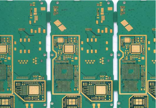
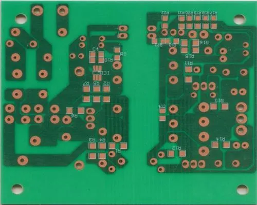
With the production of more and more complex printed circuits composed of multilayer, PCB stacking is becoming particularly important.
Good PCB stack design is essential to reduce the radiation of circuits and related circuits. On the contrary, poor accumulation may significantly increase radiation, which is harmful from a safety perspective.
What is a PCB stack?
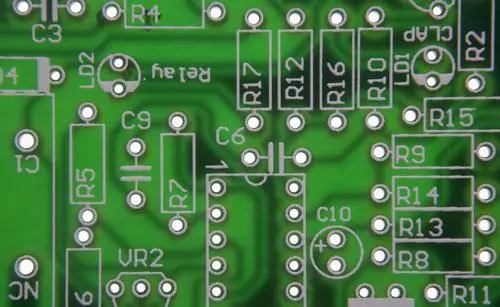
Before the final layout design is completed, the PCB stack places the PCB insulator and copper layer by layer. Developing effective stacks is a complex process. PCB connects power and signal between physical devices, and the correct layering of PCB materials directly affects its functions.
Why do I stack PCBs?
Developing PCB stack is very important for efficient PCB. PCB stack design has many advantages, because multi-layer structure can improve energy distribution ability, prevent electromagnetic interference, limit cross interference and support high-speed signal transmission.
Although the main purpose of stacking is to place multiple electronic circuits on a board through multiple layers, the structure of PCB stacking also provides other important advantages. These measures include minimizing the vulnerability of the circuit board to external noise, and reducing the crosstalk and impedance problems of high-speed systems.
A good PCB stack can also help ensure lower final production costs. By maximizing efficiency and improving the electromagnetic compatibility of the entire project, PCB stacking can effectively save time and money.
PCB stack design considerations and rules
● Number of floors
SIMple stacking may include, while more complex plates require professional sequential lamination. Although more complex, the higher number of floors allows designers to have more space for layout without increasing the risk of encountering impossible solutions.
In general, eight or more layers are required to obtain the best layer layout and spacing to maximize functionality. The use of quality planes and power planes on multilayer boards can also reduce radiation.
● Layer arrangement
The arrangement of the copper layer and insulation layer constituting the circuit constitutes the PCB overlapping operation. To prevent PCB warping, it is necessary to make the cross section of the board symmetrical and balanced when arranging each layer. For example, in an eight ply panel, the thickness of the second and seventh layers should be similar to achieve the best balance.
The signal layer should always be adjacent to the plane, while the power plane and the quality plane are strictly coupLED together. It is preferable to use multiple ground planes because they usually reduce radiation and ground impedance.
● Layer material type
The thermal, mechanical and electrical characteristics of each substrate and how they interact are critical to the selection of PCB stack materials.
The circuit board is usually composed of solid glass fiber substrate core, which can provide the thickness and rigidity of PCB. Some Flexible PCBs may be made of flexible high-temperature plastic.
The surface layer is a thin foil made of copper foil attached to the board. There is copper on both sides of the double-sided PCB, and the thickness of copper varies according to the number of layers of the PCB stack.
The top of the copper foil is covered with a layer of solder mask to make the copper wire trace contact with other metals. This material is essential to help users avoid welding jumpers in the correct position.
A screen printing layer is applied on the solder mask layer to add symbols, numbers and letters for easy assembly and better understanding of the circuit board.
● Determine wiring and through-hole
Designers should wire high-speed signals on the middle layer between layers. This allows the ground plane to provide a shield that contains radiation EMItted at high speeds from the track.
The placement of the signal level close to the plane level allows the return current to flow on the adjacent plane, thereby minimizing the inductance of the return path. There is not enough capacitance between adjacent power supply and ground plane to provide decoupling below 500 MHz using standard construction technology.
● Spacing between layers
As the capacitance decreases, a tight coupling between the signal and current return planes is essential. The power supply and ground plane should also be closely coupled.
The signal layers should always be close to each other even if they are in adjacent planes. Tight coupling and spacing between layers are critical for uninterrupted signals and overall functionality.
There are many different multilayer PCB designs in PCB stacking technology. When multiple layers are involved, a three-dimensional method must be combined to consider the internal structure and surface layout. With the high operating speed of modern circuits, careful PCB stack design is necessary to improve the distribution capacity and limit interference. A poorly designed PCB may reduce signal transmission, producibility, power transmission, and long-term reliability.


抖音二維碼

Q Q二維碼

微信二維碼
點擊
然后
聯系
然后
聯系
電話熱線
13410863085Q Q

微信

- 郵箱