鑫景福致力于滿足“快速服務(wù),零缺陷,輔助研發(fā)”PCBA訂購單需求。


PCBA方案設(shè)計(jì)
The design of PCB schematic diagram is the basis of PCB. PCB circuit SIMulation can only be carried out on the basis of a good schematIC diagram. The following is a brief introduction to the design steps of drawing the circuit schematic diagram.
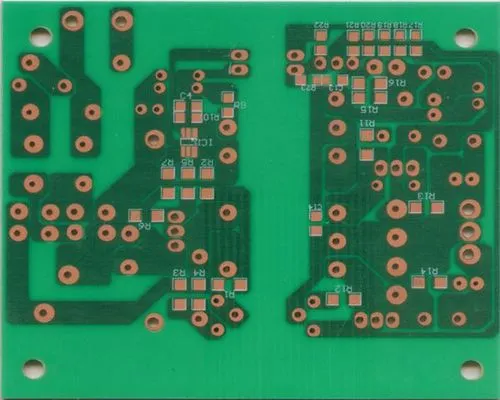
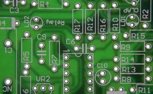
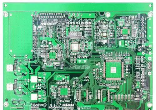
Pcb design
It includes the following 8 specifIC design steps:
(1) Create a new project and schematic file. Create a new PCB project, and the files in PCB design are included in the project.
(2) Set the paper size and working environment. Set the size of the drawing according to the complexity of the actual circuit. In the whole process of circuit design, the size of drawings can be adjusted continuously.
(3) Load a catalog. All components in the schematic are from the catalog, so load the catalog before placing the component.
(4) Place PCB components. Select components from the component library, arrange them to the appropriate position on the drawing, define and set the name and package of components, adjust and modify the position of components on the work plane according to the routing between components, etc., to make the schematic beautiful and easy to understand. (Note: When drawing with DXP, some components cannot be found in the standard component library, so you need to edit your own components.)
(5) Schematic wiring. According to the needs of the actual circuit, use various tools and instructions provided by SCH to carry out PCB wiring, and connect the devices on the work plane with wires and symbols of electrical significance to form a complete circuit schematic diagram.
(6) Electrical check of schematic diagram. After the schematic wiring is completed, you need to set the project option to compile the current project, and use the violation information inspection report provided by Protel DXP to modify the schematic.
(7) Adjustments and modifications. If the schematic has passed the electrical inspection, you can generate a network table to complete the schematic design. For general circuit design, especially for large projects, it is usually necessary to modify the circuit several tiMES before passing the electrical inspection.
(8) Generate a network table file. After completing the above steps, you can see a complete circuit schematic diagram, but to complete it, you need to generate a network table file. Network table is an important link between circuit PCB diagram and circuit schematic diagram.


抖音二維碼

Q Q二維碼

微信二維碼
點(diǎn)擊
然后
聯(lián)系
然后
聯(lián)系
電話熱線
13410863085Q Q

微信

- 郵箱