鑫景福致力于滿足“快速服務,零缺陷,輔助研發”PCBA訂購單需求。


PCBA方案設計
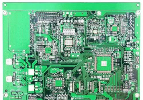
1、 Four layer PCB design drawing program:
1. Draw the circuit diagram and make the network table.
The process of drawing schematIC diagram involves the drawing of elements and the drawing of encapsulation. It is no problem to master these two kinds of drawing schematic diagrams. The elimination of errors and warnings can solve general problems. You can use hierarchical diagrams to draw complex diagrams.
Shortcuts used here: Ctrl+G (set MESh spacing), CTRL+M (measure the distance between two points)
2. pcn design board.
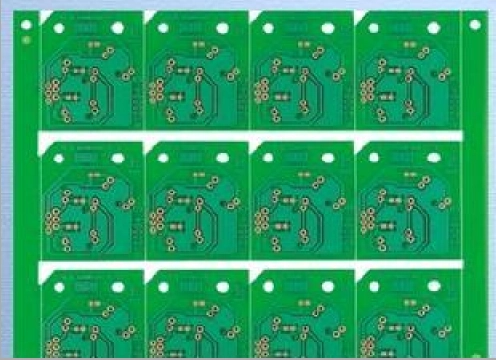
How many boards are used? Do you want to use one side elements or two sides? What is the size of the board? wait a minute
3. Set parameters.
Layout parameters and board layer parameters are basically set according to the preset values of the system, and only a few parameters are set.
4. Loading of network tables and component packages.
Note: If there is an error when drawing the schematic diagram, but the PCB layout has been designed, and you want to modify the error without affecting the PCB layout, you must do this step. Do not check Add in front of AddROOMS!!! Otherwise, it will be revised, which is really painful!!
The network table is the interface between the circuit schematic diagram editing software and the PCB design software of the printed circuit board. Only after the circuit board is loaded, can the circuit board be automatically routed.
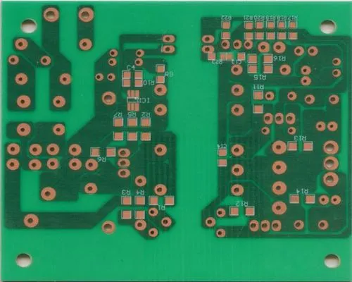
Most of them are manual layout, or automatic and manual combination.
If you want to place the component on both sides: select the device, press the left mouse button, and then press L; Or click the component on the PCB interface and modify its attribute to bottomlayer.
be careful:
The parts are evenly drained for easy installation and plug-in Welding operation. The typesetting level, reasonable position, and direction shall be paid attention to, so as to avoid being blocked and facilitate production.
6. PCB wiring
Self provided wire: manual wiring (the layout shall be planned before wiring, and the internal electrical layer shall be coordinated. The internal electrical layer shall be hidden first for PCB wiring. The internal electrical coating is generally a complete copper film. The pad and copper film have the same net name. When passing through the internal electrical layer, the system automatically connects it with the copper film. The connection mode and safety distance between the mesh copper sheet and non mesh PCB pad/via and the internal electrical layer can be set according to the regulations.


抖音二維碼

Q Q二維碼

微信二維碼
點擊
然后
聯系
然后
聯系
電話熱線
13410863085Q Q

微信

- 郵箱