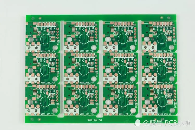
鑫景福致力于滿足“快速服務,零缺陷,輔助研發”PCBA訂購單需求。


PCBA方案設計
RF circuit PCB design process
1: Because Protel99SE is managed in the project database mode and is implICit in Windows 99, a database file should be created to manage circuit schematics and PCB layout.
2: For the design of schematic diagram, in order to realize network connection, the components used in the schematIC design must exist in the component library, or the required components must coexist in the SCHLIB storage file, and then just call the required components from it. The component library is connected according to the designed circuit diagram.
3: After the schematic design is completed, a network table for PCB design can be formed.
4: PCB proofing design PCB size and size. The shape and size of a PCB depend on the position and shape of the PCB in the product, the size and shape of the space, and the fit with other components. The shape of the PCB is drawn by the PLACETRACK command of the MECHICALLAYER layer.
5: According to the requirements of SMT, make positioning holes, eyelets, reference points, etc. on the PCB.
6: Parts manufacturing. If you need to use some special components that do not exist in the component library, you need to build the components before layout. Protel99SE components are relatively SIMple to make. Select the "MAKELIBRARY" command in the "Design" menu, enter the component production window, and then select the "NEWCOMPONENT" command in the "Tools" menu to design components. At this time, it is only necessary to draw appropriate backing paper bases at appropriate positions according to the shape and size of the actual components in the TOPLAYER layer, edit them into the required backing paper (including the shape, size, diameter, angle, etc. of the mat), and MARK the corresponding pin naMES of the mat), and then mark the corresponding pin names of the liner, Then use the PLACETRACK command to draw the largest shape of the component in the TOPOVERLAYER layer and store the component name in the component library.
The Importance of On line Testing ICT in PCB Design
DeSPIte the continuous development of competitive testing technology, online testing (ICT) is still one of the effective methods to test PCB components. The lasting appeal of ICT comes from the speed of testing, which usually lasts only a few seconds. In addition, the test is accurate. Component level error detection speeds up the diagnosis process and reduces the diagnostic proficiency. This paper discusses the importance of online testing in PCB design.
What is online testing?
ICT requires a special automatic test equipment (ATE) to perform manufacturing defect analysis (MDA). It tests each component on the PCB separately. In addition, it verifies such things as basic power supply voltage measurement, diode and transistor orientation, and passive component measurement (resistors and capacitors). It looks for open and short circuit faults.
Why is PCB design important?
In order to achieve ICT, people need to invest in a bunch of nail test fixtures and a special test program. The total cost of these testing projects exceeds $12000. Due to the high results of this non repetitive engineering load (NRE), this method is suitable for large capacity and stable design.
How to design?
In order to make full use of the test strategy, the following points should be considered when designing PCB assembly layout:
Test board access: The electrical network with "no connection" (i.e. unconnected IC pin) shall have a PCB designed test board. An exception to the traditional "through-hole" technique is the ability to detect component legs on the component weld surface. Ideally, pads should be 0.05 inches in diameter and at least 0.1 inch apart from other components. This allows the use of sturdy test pins. In addition, the pad must be at least 0.125 inches from the edge of the PCB.
Design stability: It is important before determining whether the design is stable, as these devices can be very expensive.
Bottom detection: ideally, the test pad should be located on the welding surface of the PCB. It is feasible for both parties to discuss. If needle tip detection is required, wiring and additional transmission probes will make the lamp expensive.
Welding surfaces: Unless unavoidable, there shall be no parts on the welding surfaces.
Tool holes: Remember to add tool holes on the main PCB. These tool holes enable the tool pin to position the PCB in the fixture. These holes are 3 to 4 mm in diameter and are not plated. They shall be located at the opposite angle of the diagonal, with a clear space of about 5 mm around them, so that the clamp tool pins will not be short circuited to the rails or components.
![Deep understanding of SMT technology [must see]](http://www.intomotor.com/uploadfile/ueditor/image/202211/166752938233792d.jpg)


抖音二維碼

Q Q二維碼

微信二維碼
點擊
然后
聯系
然后
聯系
電話熱線
13410863085Q Q

微信

- 郵箱