鑫景福致力于滿足“快速服務(wù),零缺陷,輔助研發(fā)”PCBA訂購(gòu)單需求。


PCBA方案設(shè)計(jì)
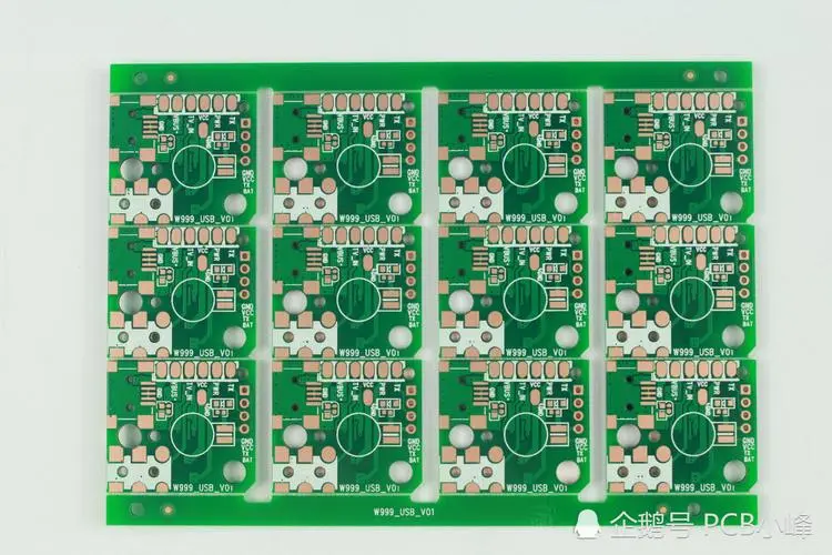
![Deep understanding of SMT technology [must see]](http://www.intomotor.com/uploadfile/ueditor/image/202211/166752938233792d.jpg)
Deep understanding of SMT technology [must see]
SMT technology originated in the 1960s and was initially developed by IBM in the United States, and then gradually matured in the late 1980s. As the name implies, SMT refers to Surface Mounted Technology, whICh is a kind of electronic circuit production technology to mount components or directly place them on the surface of printed circuit boards.
1. SMT mounting
The positions where surface mount components are required need to be flat. Generally, the welding positions with no through-hole for soldering tin, silver or gold are calLED "pads". Solder paste, a kind of sticky material composed of lead tin composition and soldering aid mixture, can penetrate stainless steel or nickel steel MESh and attach to the bonding pad with the help of a solder paste printer, or can be completed through the principle of jet printing, SIMilar to an inkjet printer. After the solder paste is printed, the circuit board will go through the picking and placing equipment and be mounted through the corresponding conveyor belt. The components to be mounted are generally placed in paper or plastic pipes and installed on the SMT mounting machine with the help of Feida. Some large integrated circuits will be transported through anti-static tray. SMT equipment takes out corresponding components from Feida and pastes them onto PCB. Since solder paste on PCB has certain viscosity, components on bonding pad have good adhesion effect.
At this time, the PCB board will be transferred to the reflow soldering furnace. The reflow soldering first has a preheating area, where the temperature of the circuit board and components rises gradually, and then enters the high temperature area. The solder paste will melt and bind the pads and components. The surface tension of the melted solder paste will keep the components in their positions without any deviation, and even the surface tension will automatically pull the slightly deviated components back to the correct position. There are many kinds of reflow soldering technologies, one is to use infrared light (called infrared reflow soldering), the other is to use hot gas convection, and the other is the most popular technology, which is to use special high boiling fluorocarbon liquid (called vapor reflow soldering). In view of environmental considerations, this technology was gradually abandoned after the introduction of lead-free regulations. Before 2008, standard air or nitrogen convection reflow welding was the mainstream. Each method has its advantages and disadvantages. In the infrared radiation mode, the Board Designer must pay attention that short components will not be shielded by high components, but if the designer knows that steam reflow or convection reflow is used in the production process, the component position will not be a factor to be considered. In the reflow stage, some unconventional or heat sensitive components need to be manually welded, but for a large number of such components, the corresponding reflow welding process needs to be completed through infrared beams or convection equipment.
If the PCB board is of double-sided design, all solder paste printing, mounting and reflow soldering processes need to be repeated once, and the components should be adhered to the designated position through solder paste or red glue. If wave soldering process is required, components need to be adhered with red glue to prevent them from falling off due to solder melting during wave soldering heating.
After the welding process is completed, the board surface needs to be cleaned to remove the rosin flux and some tin balls to prevent them from causing short circuits between components. Rosin flux is removed by fluorocarbon solvent, high ignition point hydrocarbon solvent or low ignition point solvent (such as lemon olein extracted from orange peel). The water-soluble flux is removed by ionized water and cleaning agent, and then the surface moisture is quickly removed by using the air knife. However, no cleaning process is carried out for indiscriminate mounting, that is, rosin flux will remain on the surface of PCB, which will save cleaning costs, improve production efficiency and reduce waste.
Some SMT mounting production standards, such as IPC (Association Connecting Electronics Industries), need to implement cleaning standards to ensure the cleanness of PCB boards, and even some fluxes that need not be cleaned must be removed. Correctly clear the flux, dirt and impurities that cannot be identified by naked eyes between lines. However, not all manufacturers will strictly comply with IPC standards and display them on the board, or customers will not care. In fact, the production standards of many manufacturers are stricter than IPC standards.
Finally, PCB boards need to be visually inspected to see if there are missing components, wrong direction, faulty soldering, short circuit, etc. If necessary, the defective boards need to be sent to a professional repair bench for repair, such as ICT test or FCT function test, until the tested PCB works normally.
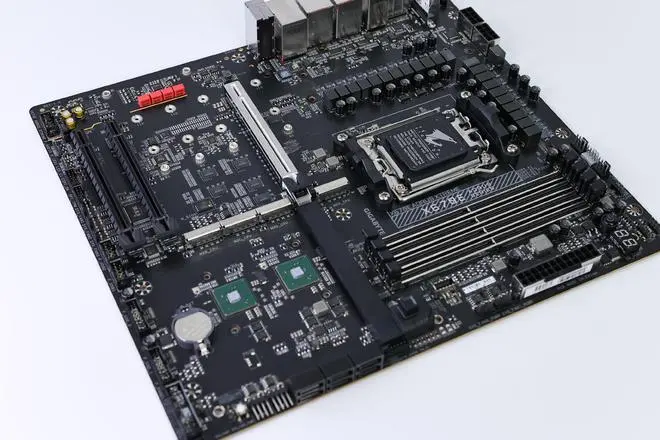
2. THT welding
tht
In this industry, there are two methods: SMD (surface mount device) and THT (through hole technology). The two technologies can be applied on the same PCB, but the piercing and inserting technology is applied to those components that are not suitable for surface mounting (such as large transformers, connectors, electrolytic capacitors, etc.).
T HT adopts components with leads. Circuit connecting wires and mounting holes are designed on the PCB. By inserting the component leads into the pre drilled through holes on the PCB, and after being temporarily fixed, soft soldering techniques such as wave soldering are used on the other side of the substrate to form reliable solder joints and establish long-term mechanical and electrical connections. The component body and solder joints are respectively distributed on both sides of the substrate. With this method, because the components have leads, when the circuit is dense to a certain extent, the problem of reducing the volume cannot be solved. At the same time, the faults caused by the proximity between leads and the interference caused by the lead length are difficult to eliminate.
In addition to the above typical SMT technology, there are many SMT chip processing processes for special packaging components, such as BGA welding, PoP process, etc., which have very complex mounting and wave soldering requirements. Interested engineers can search and understand on the Internet by themselves.


抖音二維碼

Q Q二維碼

微信二維碼
點(diǎn)擊
然后
聯(lián)系
然后
聯(lián)系
電話熱線
13410863085Q Q

微信

- 郵箱