鑫景福致力于滿足“快速服務,零缺陷,輔助研發”PCBA訂購單需求。


PCBA方案設計
As an important part of hardware PCB design, it is an absolutely important index that affects the reasonable performance of hardware circuit design. Many PCB layout engineers complete PCB wiring according to the limits of hardware engineers or Piss engineers, whICh are often referred to as "pull workers". They repeated and mechanically completed a PCB layout. After a period of time, some of them may have some experience: which should be the same length, which should be thick, which should be parallel, to ensure proper line spacing, and so on. However, they rely on so-calLED experience, many of whom know that they do not know what it is. I believe that if we want to make a breakthrough, we must expand our knowledge.
PCB layout
In other words, PCB layout engineers should not be viewed as "line workers" by others. First of all, you must have a certain degree of circuit understanding (of course, the design ability of a hardware engineer is unnecessary, if possible, it is the best); Secondly, it is necessary for SI/PI engineers to conduct pi/si analysis (of course, if possible, RF SIMulation capability is not required, which is the best).
With this knowledge, you can not only design good PCBs, but also obtain funds from hardware and SI/PI engineers, and even get advice on their circuit design from PCB design.
Not to mention, some PCB designs summarize some principles:
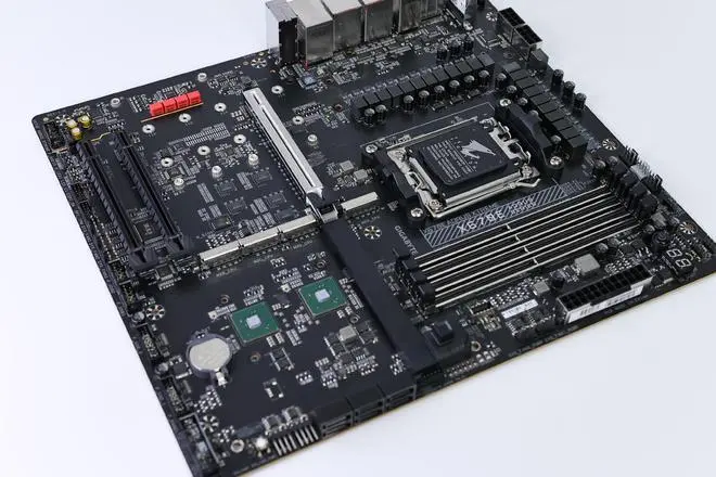
1、 About layout 1. Layout is a reasonable layout of circuit elements.
That kind of placement is reasonable. A simple principle is that the module division is very clear, that is, people can use a certain circuit basis to get your PCB and see which one is used to achieve what functions.
2. SpecifIC design steps: first, form the initial PCB file according to the schematic diagram, complete the pre layout of PCB, determine the relative PCB layout area, and then tell the structure that the structure is based on the area we give, and then give specific constraints according to the overall structure design.
3. Complete the drawing of plate edges, positioning ports and some prohibited areas according to the structural constraints, and then complete the placement of connectors. 4. Element placement principle: Generally, the main control MCU is placed in the center of the circuit board, and then the interface circuit is placed close to the interface (such as MESh, USB, VGA, etc.), and most interfaces have ESD protection and filtering processing.
The following principle is to protect the post filter first.
5. Then comes the power module. Generally, the main power module is placed at the power inlet (such as system 5V), and the discrete power module (such as module circuit power supply 2.5V) can be placed in a denser place in the same power grid according to the actual situation. 6. PCB connector is not introduced into some internal circuits.
We generally follow such a basic principle: high-speed, low-speed division, analog, digital division, interference source, sensitive receptor sub region.
7. Then, for a single circuit module, the circuit board design shall be followed in the current design. It is speculated that the entire board layout can be added and corrected.
![Deep understanding of SMT technology [must see]](http://www.intomotor.com/uploadfile/ueditor/image/202211/166752938233792d.jpg)


抖音二維碼

Q Q二維碼

微信二維碼
點擊
然后
聯系
然后
聯系
電話熱線
13410863085Q Q

微信

- 郵箱