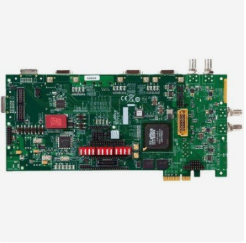
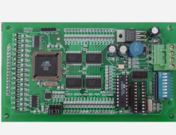
鑫景福致力于滿足“快速服務,零缺陷,輔助研發”PCBA訂購單需求。


PCBA方案設計
The best PCB design method: six things to consider when transferring PCB schematic diagram to layout design.
Initial schematIC transfer
In the process of transferring the schematic diagram to the layout environment through the netlist file, the device information, netlist, layout information and initial routing width settings will also be transferred.
The following are some recommended steps for the layout design phase:

1. Set the grid and units to the appropriate values. In order to achieve more detaiLED layout control for components and wiring, device grid, copper grid, via grid and SMD grid can be designed as 1mil
2. Set the blank area and vias of the circuit board frame to the required value. PCB manufacturers may have specific minimum or nominal recommended values for blind hole and buried hole settings.
3. Set corresponding pad/via parameters according to the capability of PCB manufacturer. Most PCB manufacturers can support SMAller vias with a drilling diameter of 10mil and a pad diameter of 20mil.
4. Set design rules as required.
5. Set customized shortcut keys for common layers, so that you can quickly switch layers (and create vias) when routing.
Handling errors during schematic transfer
A common error in the process of schematic diagram transfer is the absence or incorrect package assignment. Note:
● If a component in the schematic diagram is not encapsulated, an alarm MESsage will pop up indicating that the virtual component cannot be exported. In this case, no default packaging information will be transferred to the layout, and components will be SIMply deleted from the layout.
● If the package is transferred, but the effective package shape cannot be matched correctly, an alarm message indicating mismatch will also be generated during the transfer process.
● Correct the package assignment in the schematic, or create a valid package for any device. Correct before performing the forward dimension step to update and synchronize design information.
Updating a Design with Dimensions
Annotations are the process of transferring design changes from schematic to layout or from layout to schematic. Backward annotation (layout to schematic) and forward annotation (schematic to layout) are the key to keep the design accurate.
In order to protect the completed work, it is necessary to back up and archive the current version of schematic and layout files before any important forward or reverse annotation steps.
Do not attempt to make changes in both the schematic and the layout at the same time. Make changes to only one part of the design (either schematic or layout), and then perform the correct annotation steps to synchronize the design data.
Renumber devices
Device renumbering refers to a function that renumbers components on a PCB in a specific order. The reference labels should be sorted from top to bottom and from left to right on the PCB. In this way, it is easier to locate the device position on the board during assembly, testing and error checking.
Handle last minute device or netlist changes
It is not advisable to change PCB components or netlists at the last moment, but sometimes it is necessary to do so because of device availability problems or design errors detected at the last moment. If the component or netlist needs to be changed, it should be done in the schematic diagram, and then labeled to the layout tool through the forward direction. Here are some tips:
1. If a new device is added after the layout design starts (such as a pull-up resistor on the open drain output), then add a resistor and network to the design from the schematic diagram. After positive annotation, the resistance will be displayed outside the outer frame of the circuit board as an un laid out component, and the flying wire will be displayed to indicate the connection network. Next, move the components to the outer frame of the circuit board and conduct normal wiring.
2. Backward annotation and reference label change can work well together, such as renumbering the rear layout.
Select the positioning device by highlighting
During PCB layout, one way to browse specifIC components or routes in the schematic diagram is to use the 'highlight selection' function. This function allows you to select a component or a route (or multiple objects), and then view their positions in the schematic diagram.
This function is particularly useful when matching bypass capacitors with their corresponding IC connections. Conversely, you can locate specific components or routes in the layout while browsing the schematic.


抖音二維碼

Q Q二維碼

微信二維碼
點擊
然后
聯系
然后
聯系
電話熱線
13410863085Q Q

微信

- 郵箱