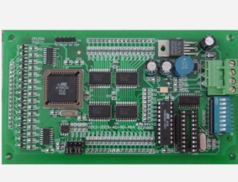
鑫景福致力于滿足“快速服務(wù),零缺陷,輔助研發(fā)”PCBA訂購單需求。


PCBA方案設(shè)計(jì)
PCB design is a manual task in many people's eyes. However, at the early stage of a scheme, I have always laid out and wired in person. Only after the finalization of the scheme, I handed over some modifICations to my colleagues, but I will also explain to them one by one why such wiring is required. I also often comment on the PCB designed by my colleagues, pointing out the missing areas, so that my colleagues have made great improvements in PCB design.

Years ago, a colleague was responsible for laying a stepping motor drive board, and the performance indicators always faiLED to meet the performance mentioned in the document. Although it could be used, the high current lost step, the high speed could not go up, and the waveform was poor, after in-depth analysis, it was found that it violated some basic principles of PCB wiring, and the performance was very good after modification. This made me feel the importance of PCB wiring again, especially that we often do high-power power supply Sensors are extremely strict with PCB wiring.
In the forum, I saw the PCB wiring problem raised by a lot of netizens. I felt the problem caused by the stepping motor wiring before. I used common sense to understand this PCB wiring. It was easy to understand, avoiding circuit loops, electromagnetic transmission lines and other highly complex things, which beCAMe more and more unclear. It basically made everyone understand what was going on, not restricted by some professional terms, and won the recognition of most netizens.
PCB wiring is to lay a road with power on signals to connect PCB components, which is like building roads and connecting cities with automobiles.
Road construction requires two lines, one for going and one for returning. The same principle applies to PCB wiring. A two line loop needs to be formed. For low-frequency circuits, it is a loop. For high-speed electromagnetic fields, it is a transmission line, such as the differential signal line. Such as USB, network cable, etc. For the impedance characteristics of transmission lines, please refer to the article "Understandable electromagnetic field theory".
It can be said that the differential signal line is an ideal model for connecting device signals. The higher the signal requirements, the closer to the differential signal line.
Double sided pcb board. Take the bottom floor as a common reference loop
When there are many sub components on a board, if they are all distributed according to differential lines, first, the area of PCB is too large, and second, 2N lines need to be distributed, which is too much work and difficult, so people put forward the concept of multi-layer PCB according to the actual needs, and the most typical is the double-sided PCB board. The bottom layer is used as a common reference loop, so that only N+1 pieces are needed for wiring, and the PCB layout is greatly reduced
The common reference loop, which is often referred to as the reference ground, for most embedded industries, the signal quality requirements are not very high after digitization, so the use of a whole layer of reference ground can reduce the board surface, improve efficiency, greatly save time, and is very popular. In fact, reducing the board surface is to shorten the length of the signal line, which can also partially offset the problem of signal quality degradation caused by the reference ground. Therefore, in practice, this PCB wiring effect introduced to the reference ground is basically close to the ideal differential line model. Today, we are all used to this way. It seems that PCB wiring is to have a layer of reference ground. There is no reason why.
In the design of double-sided boards, because there are often cross lines, the jumper needs to be switched to the stratum for cross lines. It should be pointed out that the jumper cannot be too long. If it is too long, it is easy to split the reference ground. Especially for some lines with high signal quality requirements, the reference ground at the bottom cannot be split,. Otherwise, the signal circuit will be completely destroyed and the reference ground will lose its meaning. Therefore, generally speaking, the reference stratum is only suitable for short jumpers of signal lines. The signal lines should be laid on the top layer as much as possible, or PCB boards with more layers should be introduced.
It is easy to have an impact if the roads are too close to each other. For example, when you take the high-speed rail, you can feel the impact of the train coming from the opposite side on your train. The signal line should not be too close. If the signal line is parallel to the signal line, a certain distance must be kept. This is subject to the experiment, and there should be a good reference ground at the bottom. Under low frequency and SMAll signal, the influence is generally not great, but high frequency and strong signal need attention.
For high frequency and high current PCB wiring, such as switching power supply, the most taboo is that the drive signal is interfered by the output strong current and strong voltage. The driving signal of MOS tube is easily affected by the strong output current. The two should be kept at a certain distance and not too close. In the era of analog sound, if the amplifier magnification is too high, self excitation effect will occur, for the same reason as MOS transistor.
The carrier of PCB wiring is a PCB board. Generally, the reference ground is 1mm away from the PCB board edge, and the signal line is 1mm away from the reference ground edge. In this way, the signals are constrained in the PCB board, which can reduce EMC radiation.
When there is no concept of PCB design, just think about our daily road. The two are completely consistent.
This paper describes that PCB wiring is to lay the road of power on signal to connect each PCB device


抖音二維碼

Q Q二維碼

微信二維碼
點(diǎn)擊
然后
聯(lián)系
然后
聯(lián)系
電話熱線
13410863085Q Q

微信

- 郵箱