鑫景福致力于滿足“快速服務,零缺陷,輔助研發”PCBA訂購單需求。


PCBA方案設計
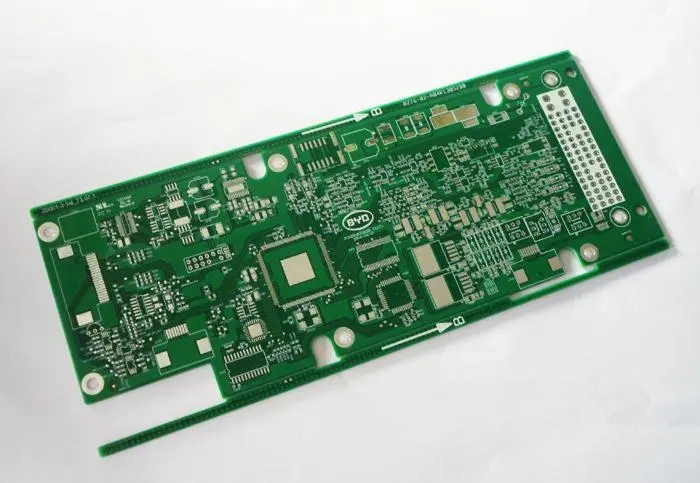
A Brief Talk on PCB electronic Manufacturer's PCB Flying Probe Testing Technology
Talking about PCB flying pin test What is flying pin test? Flying pin test is one of the methods to check the electrICal function of PCB (open and short circuit test). The flight test machine is a system for testing PCB in the manufacturing environment. Instead of using all the traditional bed of rails interfaces on the traditional online testing machine, the flying probe test uses four to eight independently controlLED probes to move to the components under test. The UUT (unit under test) is transmitted to the testing machine by belt or other UUT transmission systems. Then fix, and the probe of the tester contacts the test pad and access hole to test the single element of the UUT. The test probe is connected to the driver (signal generator, power supply, etc.) and sensor (digital multimeter, frequency counter, etc.) through the multiplex system to test the components on the UUT. When a component is being tested, other components on the UUT are electrically shielded through the probe to prevent reading interference.
Steps for making the flying probe test program:
Method I
First, import the layer file, check, arrange, align, etc., and then change the naMES of the two outer layers to fronrear. Change the names of the inner layers to ily02, ily03, ily04neg (if it is a negative film), real, rearmneg.
Second, add three layers, copy two solder mask layers and drill hole layers to the added three layers, and change their names to fronmneg, rearmneg, and mehole. Those with blind buried holes can be named met01-02., met02-05, met05-06, etc.
Third: change the copied fronmneg and rearmneg layers to the D code of 8mil round. We call fronmneg the front layer test point and rearmneg the back layer test point.
Fourth: delete the NPTH hole, find the via hole according to the line, and define the non measuring hole.
Fifth, take fron and mehole as the reference layer, and change the fronmneg layer to on. Check to see if the test points are all at the opening of the front layer line. The test point in the hole larger than 100mil shall be moved to the welding ring for testing. The test points at too dense BGA shall be misaligned. You can appropriately delete some redundant intermediate test points. The operation of the back layer is the same.
Sixth: Copy the sorted test point fronmneg to the fron layer and rearmneg to the real layer.
Seventh: Activate all layers and move them to 10,10mm.
Eighth: The output gerber file is named as fron, ily02, ily03, ily04neg, ilyo5neg, real, fronmneg, rearmneg, mehole, met01-02, met02-09, and met09-met10 layers.
Then use Ediapv software
First, export all gerber files to layer fron, ily02, ily03, ily04neg, ilyo5neg, real, fronmneg, rearmneg, mehole, met01-02, met02-09, and met09-met10.
The second is to generate a network. Net annotation of work button.
Third: Generate test files Make test programs button, input the D code of the non measuring hole.
Fourth: save,
Fifth: Set a benchMARK, and you're done. Then take it to the flying needle machine for testing.
1. Using this method to make test files often makes many test points, and cannot automatically delete intermediate points
2. The testing of holes is not well understood. Check the generated connectivity (open circuit) test points in ediapv, and there are no test points for individual holes. Another example: there is a line on one side of the hole, but there is no line on the other side. It is reasonable to test the hole on the side without a line. However, the test points generated by the ediapv transformation are random, and sometimes they are right or wrong. Depressed!
3. If the window is not opened for the anti welding of the REAR surface, you can change the name of the REAR layer to another name, so that the measuring point will not appear in the EDIAPV.
4. If there is only one side of MEHOLE with a window on both sides, but there are measuring points on both sides, you can press the make test programs button again. Note that the cursor should be positioned above the MEHOLE layer. In this way, the measuring points on the hole without window can be deleted.
5. The names of the above layers must not be wrong, otherwise you will have trouble later.
PCB manufacturers, PCB designers and PCBA manufacturers will explain PCB flying probe testing technology to you.


抖音二維碼

Q Q二維碼

微信二維碼
點擊
然后
聯系
然后
聯系
電話熱線
13410863085Q Q

微信

- 郵箱