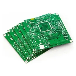
鑫景福致力于滿足“快速服務(wù),零缺陷,輔助研發(fā)”PCBA訂購(gòu)單需求。


PCBA方案設(shè)計(jì)
PCB manufacturers explain PCB flying probe test technology in detail Part II
PCB manufacturer, PCB designer and PCBA manufacturer explain PCB flying probe test technology Part II
Method II
First: import the layer file, check, arrange, align, etc., and then change the naMES of the two outer layers to fronrear. Change the names of the inner layers to ily02, ily03, ily04neg (if it is a negative film), real, rearmneg
Second, add three layers, copy two solder mask layers and drill hole layers to the added three layers, and change their names to fronmneg, rearmneg, and mehole. Those with blind buried holes can be named met01-02., met02-05, met05-06, etc.
Third: delete the LINE or other things that affect the network, and then convert the PAD corresponding to the line layer of the solder mask to PAD,
Fourth, merge the positive and negative films and retain the positive films. Change the hole attribute of MEHOLE layer to PAD, edit each layer and then output each layer in GENESIS,
The fifth is fron, ily02, ily03, ily04neg, ilyo5neg, real, fronmneg, rearmneg, meholemet01-02, met02-09, and met09 met. Enter them into Watson EZFIXTURE to define each layer, then perform network analysis, and save the run out test points.
Sixth: Save the * The Ezf file is imported into EZPROBE, and the SMAllest probe is selected to execute the minute, then C01 of the drill strip is output, and S01 is read into GENESIS.
Seventh: Change C01 and S01 to the round with D code of 8mil. First mirror C01, and then COP it to the fronmneg and rearmneg layers respectively. We call fronmneg the front layer test point and rearmneg the back layer test point. Activate all layers and move to 10,10mm.
Eighth: The output gerber file is named as fron, ily02, ily03, ily04neg, ilyo5neg, real, fronmneg, rearmneg, meholemet01-02, met02-09, and met09-met10 layers.
Then use Ediapv software
First: all the gerber fron, ily02, ily03, ily04neg, ilyo5neg, real, fronmneg, rearmneg, mehole, met01-02, met02-09, and met09-met10 layers.
The second is to generate a network. Net annotation of work button.
Third: Generate test files Make test programs button, input the D code of the non measuring hole.
Fourth: save,
Fifth: Set a benchMARK, and you're done. Then take it to the flying needle machine for testing.
My personal feeling: 1. This method is better than the first method for making test files, because Huasheng Software can delete the network midpoint, whICh can save a lot of time for testing
In general, when using EDIAPV to generate networks and test files, sometimes PCB GerBer is too dense, it is easy to short circuit. In addition, some GENESIS outputs GERBER, which cannot be recognized by EDIAPV. In this case, sometimes it will cause open circuit or short circuit.
About the time required to test the circuit board
When the tester tests circuit boards, the time required for each board is different, because the points and network of each board are different. The test time is mainly calculated according to these two items.
Making a test file will generate a report file containing the theoretical test time of the board (as shown in blue, the model is SN0800020A0).
The exact time for testing each board (usually the hard board) is when testing an OK block, and the testing time of the tester is subject to.
Generally speaking, the actual time is basically the same as the theoretical time, while the FX3000 series flying probe tester has been improved in many aspects, with improved accuracy, and the testing speed can be increased by about 20% (we have verified it through actual operation). The reasons that affect the speed of the FX3000 series flying probe tester are as follows:
1. Speed adjustment: generally, the drive speed of XY axis is adjusted to 70000, and the maximum speed is not more than 80000; Adjust the drive speed of Z-axis to 7000, and the maximum speed shall not exceed 8000, otherwise the performance of the machine will be affected, and the step will drop.
2. Shorten the waiting time after injection and needle return when measuring the plate.
3. Reduce the Z-axis lifting height: the Z-axis lifting height range is 120-360, usually set to 180-280. The larger the Z-axis lifting data, the slower the speed; On the contrary, the faster it is, but the Z-axis lifting data is too small, which may lead to scraper and other phenomena.
4. When problems occur during testing, the testing time will increase relatively. For example, if there is an open circuit in the test, when the retest is OK, the tester will automatically reset the short circuit between the open circuit network and the adjacent network, and the test time will be relatively increased; The test time will increase when an uncertain short circuit occurs. (There are many problems in the test, mainly depending on whether the quality of the PCB produced by the manufacturer is more open, whether the short circuit and surface treatment conductivity are good, and whether the setting of the operator reference point is reasonable, which requires the operator's test experience).
5. The characteristics of the board itself will also affect the test time.
For example, the test points of some boards are too close to the board edge and some flexible boards need to be fastened and supported by specific support frames. If the boards are not fixed well and shake back and forth, the Z-axis lifting height will be increased during the test, and the test time will be increased.
Cause Analysis and Solution of False Open Circuit in Flying Needle Test
printed board product problems
If the test equipment and process data are excluded, another case should be the PCB product itself has problems, mainly in warpage, solder resistance, and non-standard characters.
(1) Warpage: In order to rush for time, some production planners often omit the process of hot air leveling and directly send it to the final inspection. If not, the product warpage is greater than the allowable warpage range of the test equipment. Therefore, the process of hot leveling cannot be dispensed with, and inspection and testing personnel are required to add warpage measurement before testing.
(2) Soldering resistance: For products with severe open circuit, the measured results are not satisfactory because part of the through holes are blocked by the solder barrier layer, so the test of the adapter holes (or ensuring the hole continuity) should be avoided as far as possible during the test.
(3) Characters: Many PCB manufacturers will print characters first and then conduct electronic measurement. As long as the position of character printing is slightly offset or the precision of character film is not enough, the thin sheet sticker and small hole may be partially covered by characters. Therefore, in order to avoid open circuit caused by characters, it is equipped with thin surface sticker and small hole( Φ< 0.5). It is reasonable that the printed board with high density of thin wires should be tested by electricity before characters< span="">
Difference between flying pin test and fixture test
◆ The flying probe tester is a typical equipment that uses capacitance method to test. The test probe moves quickly point by point on the circuit board to complete the test
◆ You must first learn the standard board and read in the standard value of capacitance of each network
◆ First use the capacitance method to test, and then use the resistance method to accurately confirm when the measured capacitance is not within the acceptable range
◆ Four wire measurement is available
◆ Due to the slow testing speed, it is only suitable for testing samples with small batches
Advantages and disadvantages:
◆ The test pin is easy to be damaged
◆ Slow test speed
◆ High test density The minimum pitch can reach 0.05mm or even less
◆ No fixture cost
◆ The withstand voltage cannot be tested, and the test of high-level high-density boards is risky.
PCB manufacturers, PCB designers and PCBA manufacturers will explain the second part of PCB flying probe testing technology.


抖音二維碼

Q Q二維碼

微信二維碼
點(diǎn)擊
然后
聯(lián)系
然后
聯(lián)系
電話熱線
13410863085Q Q

微信

- 郵箱