鑫景福致力于滿足“快速服務,零缺陷,輔助研發”PCBA訂購單需求。


PCBA方案設計

The quality of PCB will affect the assembly process
After that, PCB board has been generated, and components need to be assembLED before further delivery At present, common assembly methods include wave soldering, reflow soldering and a combination of both The quality of PCB board has a great influence on the assembly quality of the three processes
1. This effect of PCB quality on reflow soldering process
1.1 The thICkness of base plate is not enough, resulting in poor welding The coating thickness of the gasket surface of the component to be installed is not enough If the thickness of tin is not enough, melting at high temperature will lead to insufficient tin and poor welding of parts and gaskets Our experience is that the tin thickness on the pad surface should be>100m ''
1.2 The liner surface is dirty, so that the tin layer is not wet If the circuit board surface is not cleaned correctly, for example, the gold plate does not pass the cleaning line, etc, Impurities will remain on the gasket surface Poor welding
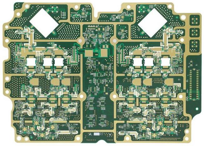
PCB board

1.3 The wet film is offset on the gasket, resulting in poor welding The pad that the component needs to be installed on the wet film offset will also cause poor welding
1.4 The gasket is incomplete, resulting in the component not being welded or firmly welded
1.5 The development of BGA pad is not clean, and there are still wet films or impurities left, which leads to Wuxi welding during installation
1.6 The plug hole at BGA is protruded, resulting in insufficient contact between BGA component and bonding pad, which is easy to open
1.7 The solder mask at BGA is too large, which causes copper exposed in the circuit connected to the bonding pad and short circuit with the BGA patch
1.8 The spacing between the positioning hole and the pattern does not meet the requirements, resulting in offset and short circuit of the printing solder paste
1.9 The green bridge between IC pads with dense IC pins is disconnected, resulting in a short circuit due to poor solder paste printing
1.10 The through-hole plug hole next to the IC protrudes, causing the IC not to be installed
1.11 The MARK holes between batteries are broken, and solder paste cannot be printed
1.12 The identification spot corresponding to the wrong fork plate is drilled by mistake, and the parts are pasted incorrectly when they are automatically attached, causing waste
1.13 The secondary drilling of NPTH hole leads to large deviation of positioning hole and deviation of solder paste printing
1.14 Light spot (next to IC or BGA), which shall be flat, frosted and free of notch Otherwise, the machine will not recognize it successfully and it will not automatically connect components
1.15 Nickel gold is not allowed to be returned to the mobile phone board, otherwise the nickel thickness will be seriously uneven Influence signal
2. Quality on wave soldering process
2.1 There is green oil in the component hole, which causes poor tin coating on the hole
For PTH with components to be inserted, annular green oil is not allowed in the hole. Otherwise, tin and lead cannot be soaked smoothly along the hole wall when passing through the tin furnace, resulting in insufficient tin in the hole. Therefore, the green oil PCB components in the hole should not exceed 10% of the hole wall area The number of holes containing green oil on the whole plate shall not exceed 5%
2.2 The coating thickness of the hole wall is not enough, resulting in poor tin coating on the hole If the coating thickness on the hole wall of the component is not enough, such as copper thickness, tin thickness, gold thickness, and ENTEK thickness, it will lead to insufficient tin (a phenomenon called "bell button" by customers) or air bubbles Therefore, in general, the copper thickness of the hole wall should be greater than 18 mm Tin thickness should be greater than 100m "
2.3 Large hole wall roughness leads to poor tin plating or faulty soldering The roughness of the hole wall is large, and the coating is uneven. In some places, the coating is very thin, which affects the effect of tin So the hole wall roughness should be <38mm.
2.4 Moisture in the hole, resulting in virtual welding or bubbles The PCB board was not dried before packaging, or was not cooled after drying, and was placed for a long time after unpacking, which would cause moisture in the hole, resulting in virtual welding or bubbles Our experience with baking boards is: under the condition of 110-1200C, tin boards are baked for 4h, gold boards and ENTEK boards are baked for 2h The service life of vacuum packaging shall not exceed 1 year
2.5 The hole pad is too SMAll, resulting in poor welding Component holes and gaskets are damaged The pad is too small, resulting in poor welding, and pad should be 4>mil
2.6 Poor tin plating caused by holes and viscera PCB boards that are not cleaned enough, such as gold boards that are not pickled, will leave dirt on holes and gaskets, which will affect the tin plating effect
2.7 The hole diameter is too small, and components cannot be inserted or welded Thickening in the hole, accumulation of tin and green oil, etc, As a result, the hole diameter is too small and the component cannot be inserted, so it cannot be welded
2.8 If the locating hole is offset, the component cannot be inserted or welded The offset of positioning hole exceeds the standard When automatically inserting components, they cannot be accurately positioned and components cannot be inserted It also cannot be welded
2.9 The rocker exceeds the standard, resulting in the component surface being immersed in tin during wave soldering For warping, it shall be controlled within 1%; The warpage of circuit board with SMI pad shall be controlled at 0.7%
3. The effect of PCB quality relates to the mixed assembly process
The influence of the quality of the PCB on the hybrid assembly process is very complicated, that is, for the board of directors, there are mounting components and plug-in components on the surface of the components, and there are mounting components on the welding surface The installation process is as follows: reflow welding of the component surface - red glue on the welding surface - red glue cured on the baking plate - wave soldering of the component surface The problems in this process have been described above, but there is a special requirement: if it is a tin spraying plate, the welding surface cannot be polytin, because if polytin is used, the parts on the welding surface will stick to the red glue It falls off when passing through the tin furnace Therefore, the tin thickness of the welding surface should be strictly controlled, and the PCB should be as flat and consistent as possible, while ensuring the tin thickness


抖音二維碼

Q Q二維碼

微信二維碼
點擊
然后
聯系
然后
聯系
電話熱線
13410863085Q Q

微信

- 郵箱