鑫景福致力于滿足“快速服務(wù),零缺陷,輔助研發(fā)”PCBA訂購單需求。


PCBA方案設(shè)計
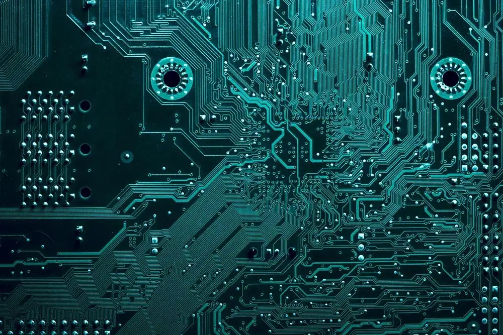
Signal processing, automatIC wiring and appearance explanation of pcb proofing
1. PCB proofing manual wiring and key signal processing
Although this paper mainly discusses the problem of automatic routing, manual routing is an important process of PCB design now and in the future. Manual routing is helpful for automatic routing tools. As shown in Figure 2a and Figure 2b, by manually routing and fixing the selected network (net), a path that can be used for automatic routing can be formed.
No matter how many key signals are, these signals can be wired first, either manually or with automatic wiring tools. The key signals usually have to be carefully designed to achieve the desired performance. After wiring, it is much easier for relevant engineers to check these signal wiring. After passing the inspection, fix these lines, and then start to automatically route the rest of the signals.
2. Automatic routing
For the wiring of key signals, it is necessary to consider controlling some electrical parameters during wiring, such as reducing the distributed inductance and EMC, etc. The wiring of other signals is SIMilar. All EDA manufacturers will provide a method to control these parameters. The quality of automatic routing can be guaranteed to a certain extent after knowing what input parameters the automatic routing tool has and the impact of the input parameters on routing.
General rules should be used to automatically route signals. By setting limiting conditions and prohibited wiring areas to limit the layers used for a given signal and the number of vias used, the wiring tool can automatically wire according to the design idea of the engineer. If there is no limit on the number of layers and vias used by the automatic routing tool, each layer will be used during automatic routing, and many vias will be generated.
After setting the constraints and applying the rules created, the automatic routing will achieve similar results as expected. Of course, some sorting work may be required, as well as ensuring the space for other signals and network routing. After part of the design is completed, fix it to prevent it from being affected by the later wiring process.
Use the same procedure to route the remaining signals. The number of wiring depends on the complexity of the circuit and the number of general rules you define. After each type of signal is completed, the constraints of other network routing will be reduced. However, many signal wiring needs manual intervention. Today's auto routing tools are very powerful, and can usually complete 100% routing. However, when the automatic wiring tool has not completed all signal wiring, it is necessary to manually wire the remaining signals.
3. The design points of PCB proofing automatic wiring include:
3.1 Change the settings slightly, and try to use multiple paths for wiring;
3.2 Keep the basic rules unchanged, try different wiring layers, different printed lines and spacing widths, as well as different line widths and different types of vias, such as blind holes and buried holes, and observe how these factors affect the design results;
3.3 Let the wiring tool handle the default networks as needed;
3.4 The less important the signal is, the more freedom the automatic wiring tool has for its wiring.
4. Arrangement of pcb proofing wiring
If the EDA tool software you use can list the signal wiring length and check these data, you may find that some signal wiring lengths with few constraints are very long. This problem is relatively easy to handle. By manual editing, the signal wiring length can be shortened and the number of vias can be reduced. In the sorting process, you need to judge which wiring is reasonable and which is unreasonable. Like manual routing design, automatic routing design can also be organized and edited during inspection.
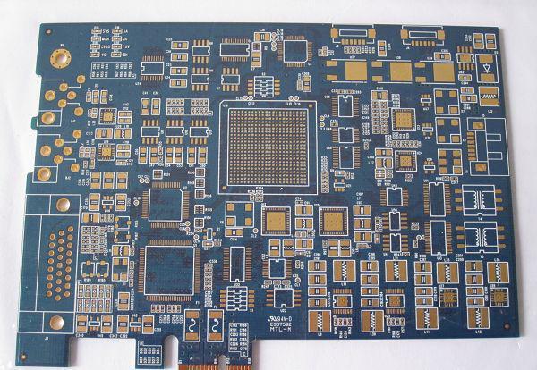
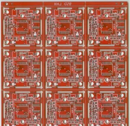
5. Appearance of pcb proofing circuit board
In the past, the design often paid attention to the visual effect of the circuit board, but now it is different. The circuit board designed automatically is not more beautiful than that designed manually, but it can meet the specified requirements in terms of electronic characteristics, and the complete performance of the design is guaranteed.
PCB manufacturers, PCB designers and PCBA manufacturers will explain the signal processing, automatic wiring and proofing appearance of pcb proofing.


抖音二維碼

Q Q二維碼

微信二維碼
點擊
然后
聯(lián)系
然后
聯(lián)系
電話熱線
13410863085Q Q

微信

- 郵箱