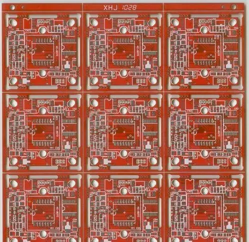
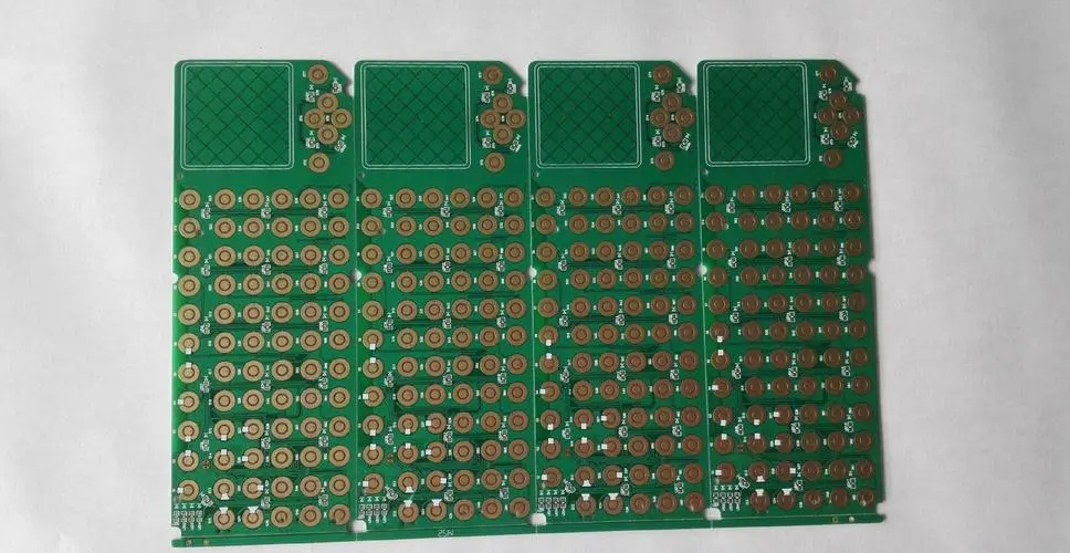
鑫景福致力于滿足“快速服務,零缺陷,輔助研發”PCBA訂購單需求。


PCBA方案設計
DetaiLED explanation of the trend of pcb proofing electronIC design
The current electronIC design of PCB proofing is mostly integrated system level design. the whole project includes both hardware design and software development. This technical feature presents new challenges to electronic engineers.
First, how to divide the system software and hardware functions reasonably in the early design stage to form an effective functional structure framework to avoid redundant cycle process;
Secondly, how to design high-performance and reliable PCB in a short time. Because the development of software largely depends on the realization of hardware, the design cycle will be shortened more effectively only if the whole machine design is passed once. This paper discusses the new characteristics and strategies of system board level design under the new technical background.
As we all know, the development of electronic technology is changing with each passing day, and the main reason for this change is the progress of chip technology. semiconductor technology is becoming increasingly physical and has reached the level of deep submicron. Ultra large scale circuits have become the mainstream of chip development. However, this change in technology and scale has brought many new bottlenecks in electronic design throughout the entire electronic industry. Board level design has also been greatly impacted. One of the most obvious changes is the great variety of chip packages, such as BGA, TQFP, PLCC and other package types; Secondly, high-density pin packaging and miniaturization packaging have become a fashion to realize the miniaturization of the whole product, such as the extensive application of MCM technology. In addition, the increase of chip operating frequency makes it possible to increase the system operating frequency. These changes will inevitably bring many problems and challenges to board level design. First of all, due to the increasing physical limit of high-density pins and pin sizes, low throughput is caused; Secondly, the timing and signal integrity problems caused by the improvement of the system clock frequency; Third, engineers hope to use better tools to complete complex high-performance designs on the PC platform. From this, we can easily see that PCB design has the following three trends:
The design of high-speed digital circuits (i.e. high clock frequency and fast edge) has become the mainstream.
The miniaturization and high performance of products must face the problem of distribution effect caused by mixed signal design technology (digital, analog and RF mixed design) on the same board.
The improvement of design difficulty leads to that the traditional design process and design method, as well as the CAD tools on PC, are not competent for the current technical challenges. Therefore, the transfer of EDA software tool platform from UNIX to NT platform has become a recognized trend in the industry.
PCB manufacturers, PCB designers and PCBA manufacturers will explain the trend of electronic design for PCB proofing in detail.


抖音二維碼

Q Q二維碼

微信二維碼
點擊
然后
聯系
然后
聯系
電話熱線
13410863085Q Q

微信

- 郵箱