鑫景福致力于滿足“快速服務,零缺陷,輔助研發”PCBA訂購單需求。


PCBA方案設計

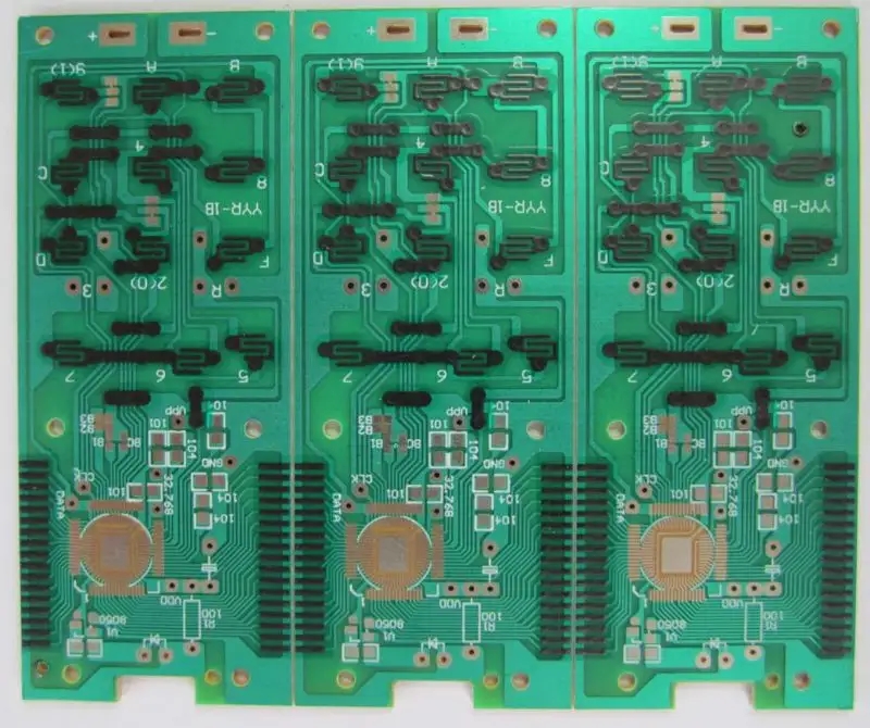
8 Suggestions for optimizing the speed of Circuit board assembly
If you are ready for circuit board assembly, here is an important consideration: make sure it is well optimized for speed The faster the circuit board is, the more beautiful its performance will be The faster the speed, the higher the effICiency It is applicable to PCB production If you can't improve the efficiency, it may lead to abnormal delivery of products
So, how to optimize PCB and assembly? Here we put forward eight suggestions. Let's take a look.
Plan ahead
The best way to optimize PCB assembly is planning. You must be clear about your requirements. From determining the target signal speed to analyzing the requirements of sensitive signals, data requirements, etc., everything should be kept safe.
DetaiLED files will help suppliers to make assembly plans and purchase required materials more quickly. Fast and accurate preparation will speed up your assembly efficiency.
In order to further organize the work and ensure the best turnkey PCB assembly, you must write down all the points from the beginning to clarify your requirements.
design technology/wiring related to schematics (to minimize wiring and other problems)
Circuit board

To ensure fast pcb assembly, attention must be paid to the schematic diagram Design schematics help to accurately describe the circuit flow and help engineers work on circuit boards
The diagram provides a clear view of the required components, clock lines, how to route differential pairs, and other SIMilar terms. And other relevant aspects. All this convenient information can help engineers better equip and help them decide the correct layout to achieve high-Speed PCB.
You can provide suppliers with clear PCB layout. When PCB suppliers get a clear PCB layout, they can make production plans more effectively. Chaotic PCB layout will lead to unclear pictures and complex structures, which will take some time to analyze. At the beginning, PCB designers are indispensable. If you have a good designer and communicate with your PCB supplier in time, it will be beneficial.
In a word, PCB schematic design is the first step to lay the foundation for high-speed PCB design.
Data and stacking requirements
You will agree with us that the performance of PCB depends largely on the PCB data and stacking requirements. In other words, if you want to realize high-speed PCB, you must use special data and cross standard PCB process.
You should have some information about Rogers and FR-4. In addition to choosing specific things, they even play a crucial role in stack structures.
Best practices related to stacking include orienting high-speed signals on the inner layer between planes, locating plane layers near signal layers, using multiple ground planes in the layer stack, and so on. All of these practices can significantly optimize PCB speed. In addition, accurate and direct data requirements can quickly realize PCB assembly.
Component Picking and Placement
Another best practice that you must follow when designing and assembling PCBs. Follow a proven strategy related to high-speed PCBs, rather than reinventing the wheel. Some of the best practices when placing components include placing them at key power locations or placing individual circuits in ducts that help improve the overall speed of the course.
Before assembling the PCB, you need to check the BOM file to ensure that each step is correct. We need to ensure that the PCB production is consistent with the BOM file to avoid rework. Save time and complete work efficiently.
Find ways to shorten the time frame for purchasing components
Finding the right components at the right time to meet most needs is critical. Look for manufacturers who can provide you with accurate quotations within one day and complete the turnkey process within 3-5 working days.
You can send the BOM file to the PCB supplier several days in advance. Some suppliers can provide one-stop services, including procurement materials. The information you need can be provided to them and used for PCB assembly, and the files can be prepared in advance.
To ensure that your PCB optimizes speed correctly, make sure you purchase components from reputable suppliers in the industry.
Pad and pin size
The selection of pad and pin size will affect the speed of PCB assembly and PCB function. So you need to pay special attention to this.
Pad and pin size and installation method. When designing PCB, you should communicate with PCB designer in detail. Under the same conditions, if we can generate the same function, we can choose the simplest function. It can help PCB assembly in the later stage and perform faster. Complex pad and pin sizes will affect the aesthetics and speed of PCB assembly.
Design tips:
Although standard PCB practices may recommend using larger pads, you should avoid doing so if you are developing high-speed circuits. It is strongly recommended that the pad size be limited to 0-5% of the component lead size. It will provide more space to place other differential pairs, such as integrated circuits and FPGAs. All of these help to optimize the speed of the circuit board appropriately.
Cooperation in production process
In order to achieve high-speed PCB assembly, proper cooperation is essential. The person who drew the sketch may not be the person who is assembling. In this regard, it is necessary to have good communication within the team and ensure that everything is normal.
Check with PCB suppliers to ensure that the contact information is unblocked, so that they can be contacted in time in case of any problems. The supplier is directly connected with the production factory. The efficient assembly of this PCB is inseparable from our timely communication, which is very important. For example, if you need to change data temporarily, please inform your PCB supplier in time so that you can make changes quickly and effectively. Avoid rework after PCB assembly.
Selecting large and medium-sized plants can ensure the efficiency of assembly lines.
Ultimately, the speed of PCB assembly depends on your choosing the right factory. Ideally, it will help if you decide to go to large and medium-sized plants to ensure maximum efficiency.
Each department of the factory has professional staff. This will ensure that you are not unprofessional and lose efficiency. Under normal circumstances, each process of a large manufacturing organization has a professional department. There is no doubt that it proves complete professionalism and efficiency.
You can rest assured that not only the efficiency of PCB is optimized, but also the design and assembly can be carried out according to the specified time frame without delay. This is critical, especially if you have other processes that rely on PCB assembly.
In short
By following the above steps, you will be able to optimize PCB components plan carefully, use the right information, and use the appropriate stacking technology The correct pad and pin size also play a vital role in determining the speed of the PCB


抖音二維碼

Q Q二維碼

微信二維碼
點擊
然后
聯系
然后
聯系
電話熱線
13410863085Q Q

微信

- 郵箱