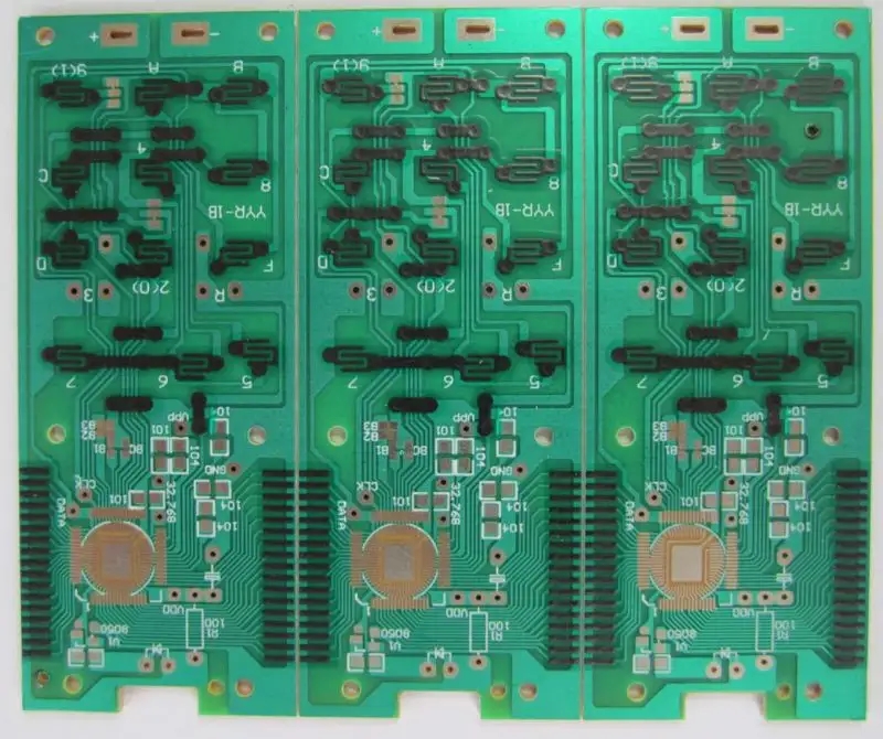
鑫景福致力于滿足“快速服務,零缺陷,輔助研發”PCBA訂購單需求。


PCBA方案設計
NovICe Xiaobai learns to draw pcb boards in 5 days. Come and see
circuit board manufacturing, circuit board design and PCBA processing manufacturers explain to you that novice Xiaobai learns to draw PCB boards in 5 days. Come and see
1. Software installation: This example installs AD17.1.
2. Basic concepts to master before drawing PCB board:
2.1 A complete PCB file generally includes project file (. PrjPCB), pcb file (. PcbDoc), schematic file (. SchDoc), and pcb package library file (. PcbLib).
Briefly introduce the relationship between them: the project document is a general document, and other related documents are included in it. The Pcb file is most of the files that we need to draw, and it is also a file for the processing pcb manufacturer. The schematic file requires us to connect the electrical components of the pcb board according to it. The PCB packaging library file is a library of the size of the bonding pads of the components that we need to weld on the board (we can also export the pcb packaging library we need according to the drawn PCB board).
2.2 Before drawing the circuit board, I should have a basic understanding of some basic concepts and operations of the pcb board. According to my initial learning experience, I listed several concepts that I thought I needed to know.
Hierarchy concept: pcb board has different layers, which are introduced one by one as follows:
2.2.1 Signal layer
The signal layer is mainly used to lay out the wires on the circuit board, and it is also the main operation layer for us to draw the PCB diagram, such as the top layer, the bottom layer, and 30 MidLayers.
2.2.2 Internal plane layer
This type of layer is only used for multilayer boards, mainly for arranging power lines and grounding wires We call it double layer board, four layer board and Six layer board, generally referring to the number of signal layers and internal power/ground layers.
2.2.3 Mechanical layer
It is generally used to set the overall dimensions, data MARKs, alignment marks, assembly instructions and other mechanical information of the circuit board.
2.2.4 Solder mask layer
Apply a layer of paint, such as solder mask, on all parts outside the bonding pad to prevent tin coating on these parts. The solder mask is automatically generated for matching pads during the design process.
2.2.5 Keep out layer
It is used to define the area where components and wiring can be effectively placed on the circuit board. Draw a closed area on this layer as the valid routing area. You cannot automatically layout and route outside this area.
2.2.6 Silkscreen layer
The silk screen layer is mainly used to place printed information, such as the outline and annotation of components, various annotation characters, etc., to facilitate the annotation on PCB boards during assembly and maintenance, such as resistance serial number and size.
2.2.7 Multi layer
Pads and through-hole on the circuit board need to penetrate the whole circuit board to establish electrical connection with different conductive graphic layers. Therefore, the system has set up an abstract layer - multilayer. Generally, pads and vias must be set on multiple layers. If this layer is closed, pads and vias cannot be displayed.
2.2.8 Drill layer
The drilling layer provides the drilling information during the manufacturing process of the circuit board (such as the pad, through hole drilling is required). Protel 99 SE provides two drilling layers, namely, Drillgrid and Drill drawing.
2.3 Some basic operation concepts of drawing pcb board
2.3.1 Copper laying: If there are many PCB floors, such as SGND, AGND, GND, etc., the most important "ground" shall be used as the reference for independent copper coating according to the different positions of the PCB surface, that is, the ground shall be connected together.
The benefits are:
1) Reduce ground wire impedance and improve anti-interference capability;
2) Reduce voltage drop and improve power efficiency;
3) Connecting with the ground wire can also reduce the loop area.
4) In order to keep PCB from deforming as much as possible during welding, most PCB manufacturers also require PCB designers to fill the open area of PCB with copper sheet or grid shaped ground wire.
2.3.2 Pad: used to realize the electrical connection between components and PCB board. The through-hole of the pad is used to weld pins of in-line components.
2.3.3 Through hole: used for layer switching in wiring process to achieve the required electrical connectivity.
2.3.4 Flying line: the line shown in the electrical connection relationship between components when we are making layout, which is convenient for layout.
So far, we have almost started our journey of drawing circuit boards.
2.3.5 Common shortcut keys:
Flying wire connection display N
Single layer display Shift+s
Press L while dragging the device to switch between the front and back of the device placement position
Place vias Shift+xtrl+F2
More shortcut keys can be set by Baidu or yourself.
3. Drawing steps:
3.1 Create a project and create a new "PrjPCB" file.
3.2 Add the existing schematic diagram and package library to the project.
3.3 Determine the area size of the pcb board (after drawing the board size on the keep out layer, select the wireframe, design the board shape, and select the shortcut key DSD according to the selected object definition)
3.4 Schematic compilation, check and troubleshooting
3.5 The matching import of packaging library and schematic diagram is allowed until there is no error
3.6 Then there is the specific layout and wiring, which can be done from beginning to end in combination with the video screen.
3.7 Rule check: it is very important to check the rules before drawing the pcb board to avoid mistakes. It is explained in the video screen. Prepare to follow with new common rules.
Previous: What subjects do I need to learn to design PCB by myself?
Circuit board manufacturing, circuit Board Design, PCBA processing manufacturers will explain to you that novice Xiaobai learns to Draw PCB boards in 5 days. Come and see.


抖音二維碼

Q Q二維碼

微信二維碼
點擊
然后
聯系
然后
聯系
電話熱線
13410863085Q Q

微信

- 郵箱