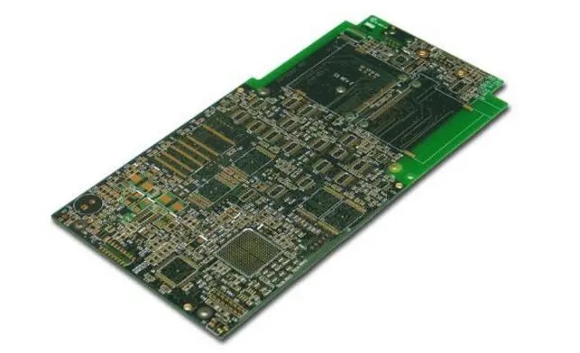
鑫景福致力于滿足“快速服務(wù),零缺陷,輔助研發(fā)”P(pán)CBA訂購(gòu)單需求。


PCBA方案設(shè)計(jì)
New Pulse Electroplating Technology and PCB Design Cut off Interference Propagation
PCB manufacturers, PCB designers and PCBA manufacturers will explain the new pulse electroplating technology and PCB design to cut off interference propagation
Pulse electroplating technology, whICh has long been used in electroforming process, is a relatively mature technology. However, a large number of process tests must be carried out in the application of high aspect ratio SMAll hole electroplating. Because the pulse power supply is different from the general DC power supply, it makes the rectifier open/close at the speed of US through a switching element to provide pulse signals to the cathode. When the rectifier is in the off state, it is more effective than DC to supplement copper ions to the boundary layer in the hole, thus making the deposition layer of the printed circuit board with high aspect ratio more uniform. At present, the developed pulse rectifier has been applied to the fully enclosed horizontal electroplating production line, and the application effect has achieved reMARKable economic and technical results.
The "timing counter pulse" is used to make the current alternately conduct positive plating and reverse plating (i.e. anodic dissolution) according to the time ratio in the power supply mode, which makes it difficult to obtain the corresponding copper layer thickness in the conventional power supply mode. When the printed circuit board on the cathode is in reverse current, the copper layer in the high current density area of the hole can be rapidly dissolved. Due to the effect of additives, the effect on the low current density area is very small, so the thickness of the copper layer in the hole and the thickness of the copper on the board will gradually become equal.
Introduction to Common Measures for Cutting off Interference Propagation Path in PCB design
Reasonable Layout of components
(1) Fully consider the influence of power supply on MCU. If the power supply is well done, the anti-interference of the whole circuit will be more than half solved. Many single chip computers are very sensitive to power supply noise. To reduce the interference of power supply noise to single chip computers, filter circuits or voltage regulators should be added to the power supply of single chip computers. For example, magnetic beads and capacitors can be used to form a π - shaped filter circuit. Of course, 100 Ω resistors can also be used to replace magnetic beads when conditions are not demanding.
(2) If the I/O port of the single chip microcomputer is used to control noise devices such as motors, isolation shall be added between the I/O port and the noise source (π filtering circuit shall be added). To control noise devices such as motor, isolation shall be added between I/O port and noise source (π filtering circuit shall be added).
(3) Pay attention to the design and wiring of crystal oscillator PCB. The crystal oscillator shall be as close as possible to the pin of the microcontroller, and the clock area shall be isolated by the ground wire. The crystal oscillator shell shall be grounded and fixed. This measure can solve many difficult problems.
(4) The circuit board shall be reasonably partitioned, such as strong and weak signals, digital and analog signals. Try to keep the interference sources (such as motors and relays) away from the sensitive elements (such as SCM).
(5) The digital area shall be isolated from the analog area with a ground wire. The digital ground shall be separated from the analog ground, and finally connected to the power supply ground at one point. The PCB design and wiring of A/D and D/A chips are also based on this principle. The manufacturer has considered this requirement when allocating the pin arrangement of A/D and D/A chips.
(6) The ground wire of single chip microcomputer and high-power device shall be grounded separately to reduce mutual interference. High power devices shall be placed on the edge of the circuit board as far as possible.
(7) Anti interference components such as magnetic beads, magnetic rings, power filters and shielding covers are used in the I/O ports, power lines, circuit board connecting lines and other key areas of the microcontroller, which can significantly improve the anti-interference performance of the circuit.
Improve the anti-interference performance of sensitive devices
Improving the anti-interference performance of sensitive devices refers to the method of minimizing the pickup of interference noise and recovering from abnormal state as soon as possible from the sensitive devices.
The common measures to improve the anti-interference performance of the sensitive devices are as follows: (1) The area of the loop shall be minimized during PCB design and wiring to reduce the induced noise.
(2) When designing PCB wiring, the power cord and ground wire should be as thick as possible. In addition to reducing the voltage drop, it is more important to reduce the coupling noise.
(3) For the idle I/O port of the microcontroller, do not hang in the air, but ground or connect to the power supply. The idle terminals of other ICs are grounded or connected to the power supply without changing the system logic.
(4) The use of power supply monitoring and watchdog circuits for SCM, such as IMP809, IMP706, IMP813, X25043, X25045, can greatly improve the anti-interference performance of the entire circuit.
(5) On the prEMIse that the speed can meet the requirements, the crystal oscillator of the single chip microcomputer shall be reduced as far as possible and the low-speed digital circuit shall be selected.
(6) IC devices shall be directly welded to the circuit board as much as possible, and IC sockets shall be used less. PCB manufacturers, PCB designers and PCBA processors will explain the new pulse electroplating technology and PCB design to cut off interference propagation.


抖音二維碼

Q Q二維碼

微信二維碼
點(diǎn)擊
然后
聯(lián)系
然后
聯(lián)系
電話熱線
13410863085Q Q

微信

- 郵箱