鑫景福致力于滿足“快速服務(wù),零缺陷,輔助研發(fā)”PCBA訂購單需求。


PCBA方案設(shè)計(jì)
The overall idea of circuit board design layout is to consider the overall beauty on the basis of meeting the electrICal and mechanical structure requirements of the product. On a PCB, the layout requirements of components should be balanced and orderly.
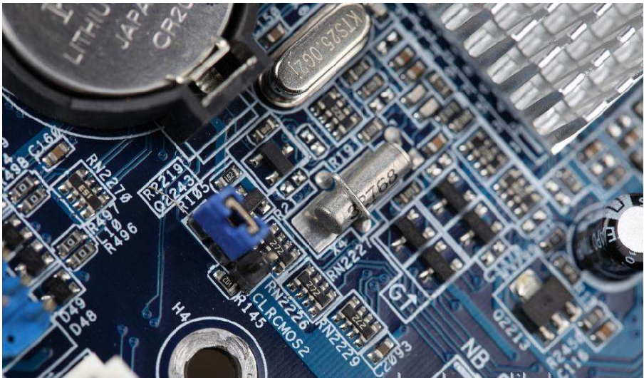
1. The size of the printed board must conform to the size of the processing drawing, meet the requirements of the pcb design and manufacturing process, and place the MARK point.
2. Is there any conflict between components in two-dimensional and three-dimensional space in PCB design?
3. Can PCB layout be dense, orderly and uniformly arranged? Can you finish all the cloth?
4. Can components that need to be changed frequently in pcb design be easily changed? Can the plug-in board be easily inserted into the device?
5. Is there a proper spacing between the thermal element and the heating element?
6. Is it convenient to adjust the adjustable components?
7. Is a radiator instalLED in the center where heat dissipation is required? Can the air flow be smooth?
8. Is the signal flow smooth and the interconnection shortest?
9. Is there any contradiction between plugs, sockets, etc. and mechanical design?
10. The buzzer shall be far away from the cylindrical inductor to prevent the distortion of interference sound.
11. Fast devices such as SRAM should be as close to the CPU as possible.
12. In the pcb design, the devices powered by the same power supply should be placed together as much as possible.
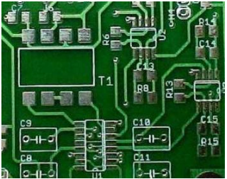
pcb design wiring:
1. The pcb design wiring should have a reasonable direction: such as input/output, AC/DC, strong/weak signal, high frequency/low frequency, high voltage/low voltage, etc. Their direction should be linear (or separate), and should not be merged with each other. The purpose is to avoid mutual interference. The best way is to follow a straight line, but it is not easy to complete in general, to prevent circular routing. The request for DC, SMAll signal and low voltage can be lower. The side lines of input end and output end shall be protected from adjacent parallelism to avoid reflection interference. If necessary, ground wires shall be added for isolation, and the wiring of two adjacent layers shall be perpendicular to each other, which may cause parasitic coupling.
2. Select the grounding point: common grounding is required under normal conditions, and digital grounding and analog grounding are connected at the power input capacitor.
3. Reasonably arrange power filter/decoupling capacitors: arrange these capacitors as close to these PCB components as possible, and they will not work if they are too far away. The decoupling capacitance of SMT chip devices should be located at the device belly on the other side of the board. The power and ground should pass through the capacitance before entering the chip.
4. The lines are exquisite: the lines that can be made wide should never be made thin; High voltage and high frequency lines shall be round and smooth without sharp chamfers, and right angles shall not be used when turning, generally 135 degrees. The ground wire should be as wide as possible, and it is better to apply large area copper coating, which can greatly improve the docking point problem. The number of wire passing holes shall be minimized to reduce the density of parallel lines.
5. The width of power supply and ground wire shall be widened as much as possible. It is better that the ground wire is wider than the power wire. Their relationship is: ground wire>power wire>signal wire.
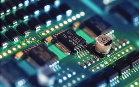
6. Common ground disposal with analog circuits. Nowadays, many PCB designs are no longer single functional circuits (digital or analog circuits), but are composed of digital circuits and analog circuits. Therefore, when wiring, it is necessary to consider the mutual interference between them, especially the noise interference on the ground wire.
The frequency of digital circuit is high, and the sensitivity of analog circuit is strong. For signal lines, the high-frequency signal lines should be as far away from sensitive analog PCB circuit components as possible. For ground wires, the integrated PCB only needs one node to the outside world. Therefore, it is necessary to stop dealing with the problem of digital and analog common ground in the PCB. In practice, the digital ground and analog ground inside the board are separated from each other, It is only at the interface between PCB and the outside world (such as connector number). There is a short circuit between digital and analog.


抖音二維碼

Q Q二維碼

微信二維碼
點(diǎn)擊
然后
聯(lián)系
然后
聯(lián)系
電話熱線
13410863085Q Q

微信

- 郵箱