鑫景福致力于滿足“快速服務,零缺陷,輔助研發”PCBA訂購單需求。


PCBA方案設計
We all know that there are many procedures from the planned feeding to the last step in the production of HDI circuit boards, one of whICh is calLED browning. Some people may ask what is the role of browning? What's the difference between it and blackening?
Browning and blackening in the HDI circuit board manufacturing process are both to increase the bonding force between the original board and PP. If the browning is not good, the oxidation surface of the HDI circuit board will be layered, the inner layer will not be etched cleanly, and the coating will be infiltrated.
The browning effect of HDI circuit board has the following three aspects:
Remove the grease and sundries on the surface to ensure the cleanness of the board surface;
2. After browning, it must be pressed within a certain period of time to avoid water absorption of browning layer, which may lead to plate bursting
3. After browning, there will be a layer of uniform fuzz on the copper surface of the substrate, so as to increase the bonding force between the PCB substrate and PP and avoid problems such as layered bursting.
There are two major differences between browning and blackening of HDI circuit boards:
1、 The SIMilarities between browning and blackening of HDI circuit boards are as follows:
A. Increase the contact area between copper foil and resin, and increase the binding force between them;
B. Increase the wettability of copper surface between flowing resins, so that the resins can flow into each dead corner and have stronger adhesion after hardening;
C. A fine passivation layer is formed on the copper surface to prevent the hardener from reacting with copper under high temperature and high pressure to generate water, resulting in plate explosion.
2、 Differences between browning and blackening of HDI circuit boards:
1. The thickness of blackened villus is different from that of browning villus;
2. The black liquid medicine is more difficult to control than the brown liquid medicine;
3. The blackened liquid medicine is more expensive than the browning liquid medicine in terms of price;
4. The micro etching rate of the blackening solution is higher than that of the browning solution;
5. Quality: The surface roughness of the blackened HDI circuit board is relatively large. If the inner line is slightly scratched or patched, the blackened HDI circuit board can cover up well, but the browned HDI circuit board cannot.
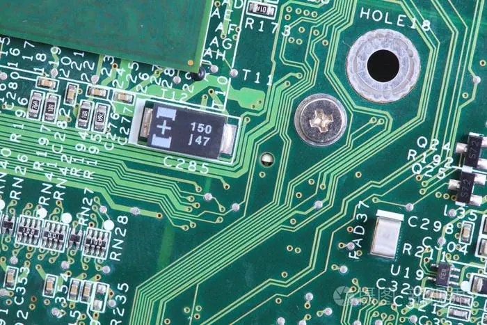
What are the common reasons for copper rejection of PCB?
In the manufacturing process of PCB, the copper wire of PCB often falls off, which is also known as copper throwing, thus affecting the product quality. So, what are the common reasons for copper rejection of PCB?
1、 PCB process factors:
1. Copper foil is excessively etched. The electrolytic copper foil used in the MARKet is generally single-sided zinc plating (commonly known as ashing foil) and single-sided copper plating (commonly known as reddening foil). The common copper rejection is generally more than 70um of ashing foil. There is basically no batch copper rejection for reddening foil and less than 18um of ashing foil.
2. In PCB process, local collision occurs, and the copper wire is separated from the substrate by external mechanical force. This defect is characterized by poor positioning or orientation, and the detached copper wire will have obvious distortion, or scratches/impact marks in the same direction.
3. The PCB circuit design is unreasonable. If the circuit is designed too thin with thick copper foil, it will also cause excessive etching of the circuit and copper throwing.
2、 Reasons for PCB laminate manufacturing process:
Under normal circumstances, as long as the high temperature section of the laminate is hot pressed for more than 30min, the copper foil and the prepreg will be basically bonded, so the bonding will not affect the bonding force between the copper foil and the substrate in the laminate generally. However, in the process of laminating and stacking, if PP is polluted or the rough surface of copper foil is damaged, the bonding force between copper foil and substrate after lamination will be insufficient, resulting in positioning (only for large plates) or sporadic copper wire falling off.
3、 Reasons for raw materials of laminate:
1. Ordinary electrolytic copper foil is the product that has been galvanized or coppered by the wool foil. If the peak value of the wool foil is abnormal during production, or the coating crystal branch is poor during galvanizing/copper plating, resulting in insufficient peel strength of the copper foil itself. When the defective foil is pressed into a PCB and inserted in the electronics factory, the copper wire will fall off under the impact of external forces.
2. Poor adaptability of copper foil and resin: wh PCB en PCB is used to produce laminate, the copper foil does not match the resin system, resulting in insufficient peeling strength of the sheet metal foil, and poor copper wire falling off may also occur during plug-in.


抖音二維碼

Q Q二維碼

微信二維碼
點擊
然后
聯系
然后
聯系
電話熱線
13410863085Q Q

微信

- 郵箱