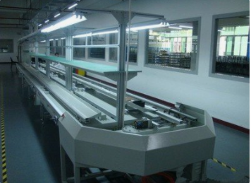
鑫景福致力于滿足“快速服務,零缺陷,輔助研發”PCBA訂購單需求。


PCBA方案設計
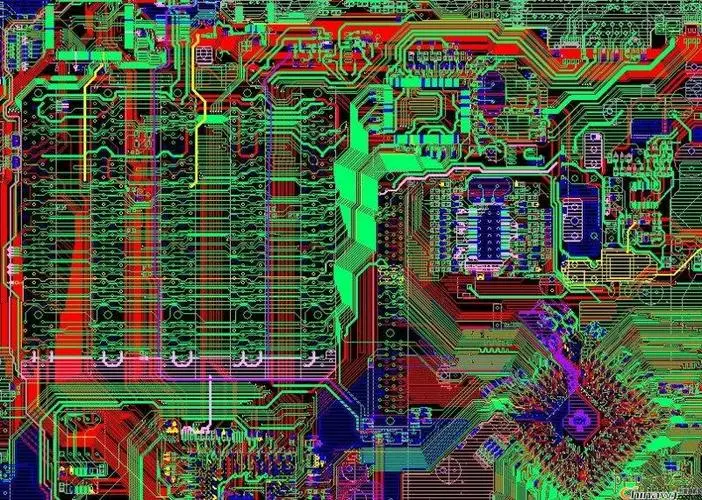
It is a recognized rule that in all analog circuit printed circuit boards, the signal line should be as short as possible, because the longer the signal line, the more inductive and capacitive contributions in the circuit, whICh is undesirable. The reality is that it is impossible to make all the signal lines as short as possible. Therefore, the first thing to consider when wiring is the signal lines that are most likely to cause interference.

In the analog circuit PCB, the signal line can complete various functions, such as signal input, feedback, output and providing reference signal. Therefore, for different applications, signal lines must be optimized in various ways. However, there is a recognized rule that in all analog circuit printed circuit boards, the signal line should be as short as possible, because the longer the signal line, the more inductive and capacitive contributions in the circuit, which is undesirable. The reality is that it is impossible to make all the signal lines the shortest. Therefore, the signal lines that are most likely to cause interference should be considered first when PCB wiring.
Pay special attention to the wiring of signal wires in the following PCB circuits:
1) High frequency amplifier/oscillator;
2) Multi stage amplifier, especially the amplifier with high output power;
3) High gain DC amplifier;
4) SMAll signal amplifier;
5) Differential amplifier.
1. High frequency amplifier/oscillator
If the wiring of the printed circuit board of the high-frequency amplifier is unreasonable, the bandwidth of the amplifier will be reduced. This is because a large capacitance will be formed between two close ground wires and signal wires, which together with the output resistance will form a low-pass filter. This low-pass filter reduces the amplifier bandwidth. At the same time, if the input signal line and the output signal line are close to each other, the feedback signal will cause oscillation. In order to avoid these problems, there should be enough space between the above conductors.
Electronic circuit designers usually have such a common experience that if a high-frequency amplifier is designed, it will actually produce oscillation. A SIMilar problem will be encountered in the layout of the oscillator, which does not oscillate according to the designed frequency. This problem is caused by the capacitive coupling between signal lines. Therefore, it is important to reduce the coupling capacitance between signal lines in PCB layout.
2. Multi stage amplifier with high power output
If the power line and ground wire are too long, the multistage amplifier is easy to generate low-frequency oscillation. Due to the resistivity of the wire itself, the large current caused by the high power output will flow through these wires. This problem can be solved by adding a large enough capacitor between the power supply and the ground to form a power decoupling circuit. Or, separate power supply and ground wire are provided for different amplification stages, so that there is no common power supply and ground wire access.
3. High gain DC amplifier
High gain DC amplifiers are usually used for small signal amplification. When devices such as transistors or DC amplifiers are welded on the printed circuit board, thermocouples will be formed at the connection between the copper cylinder and the device pins, thus generating different alternating voltages and forming an interference signal to the amplifier. In order to minimize the temperature change rate around the input stage of the DC amplifier and keep it constant, it is recommended to enclose the input stage with an isolation device to avoid the impact of air flow around it.
4. Micro signal amplifier
The signal amplifier processes tiny signals, including the following two types.
(1) High impedance (low current) amplifier
In this amplifier, there is capacitive coupling between two adjacent signal lines, which will seriously affect the performance of the circuit, and even cause low-level signals to be covered. Capacitive coupling between two conductors in a high impedance circuit. In order to reduce coupling, it is recommended to keep enough distance between signal lines with high impedance and other interfering signals. Generally, the distance shall be at least 40 tiMES the width of the signal line.
In any case, the capacitance to ground of the low-level signal line should be high to reduce the coupling voltage. This means that the low-level signal conductor should be close to the ground wire. If there is not enough width between low-level signal lines, a ground wire can be laid between them to reduce coupling.
When the amplifier uses photocell or chEMIcal cell as the power supply, the power impedance can reach millions or even hundreds of millions of ohms. If the printed circuit board is not fully cleaned after etching, the electrolyte left on the surface of the printed circuit board will produce a large resistance between adjacent wires. Even if the printed circuit board is completely cleaned, there is still a leakage resistance of no more than 10120. Moreover, these resistances cannot be equisquare, so that the resistance between two adjacent wires may be higher than that between two wires far away. Therefore, the input of low level I1 V (current/voltage) converter should be protected on both sides of the printed circuit board with a protective loop, which should be connected to the point of equipotential with the total connection point. If this is done, the precise value of the leakage resistance is not so important, because the difference voltage added to it is already very small.
Plated through-hole cannot be used for high impedance amplifier PCB. The volume resistivity of printed circuit board materials is lower than the surface resistivity, so it is difficult to install protective rings on the substrate. The best way is to connect the terminal of the high impedance amplifier to the Teflon insulator instead of the printed circuit board wire.
(2) Low impedance (low voltage) amplifier
In a low impedance circuit, it is possible to generate induced voltage because there is inductive coupling or magnetic field in the circuit. This interference can be reduced to a certain extent by the following methods:
1) Keep a sufficient distance between the high-level AC signal line and the low-level signal line;
2) Lay ground wire near signal line;
3) Avoid forming a grounding loop to prevent external magnetic fields from interfering with low-level signals.
5. Differential amplifier
The differential amplifier only amplifies the difference between two signals, while the common voltage signal will not be amplified. If the design of differential amplifier and printed circuit board is unreasonable, when the signal level is low, the common voltage will produce a small differential interference signal. The input impedance of differential amplifier is high, and the imbalance of any input parameters will cause great interference to the circuit. Therefore, in PCB design, the amplifier must be completely symmetrical in physical structure.
There is a definite leakage resistance at the input of differential amplifier, which can cause unbalanced voltage offset. This problem can be solved by adding protective devices in the input circuit. The protective device encloses the signal line. If it can maintain the same voltage with the low level terminals of the two input signal lines, it will cause an increase in the effective resistance. This device can ensure that the level of the signal source terminal and protective body is the same as the low level terminal of the signal source. The protective wire should form a circle, enclose the signal wire from the input end to the input connection point of the amplifier, and connect it with the protective device of the equipment, which is an effective method for processing low-level differential signals. In addition, the printed circuit board substrate of small signal differential amplifier is more suitable for using epoxy glass material, which helps to reduce leakage current.
The basic knowledge of PCB design
10-23,2022


抖音二維碼

Q Q二維碼

微信二維碼
點擊
然后
聯系
然后
聯系
電話熱線
13410863085Q Q

微信

- 郵箱