鑫景福致力于滿足“快速服務(wù),零缺陷,輔助研發(fā)”PCBA訂購(gòu)單需求。


PCBA方案設(shè)計(jì)
The basIC knowLEDge of PCB design Printed Circuit Board (PCB) will appear in almost every kind of electronic equipment. If there are electronIC parts in a certain device, they are also embedded in PCB of different sizes. In addition to fixing various SMAll parts, the main function of the PCB is to provide the electrical connection between the upper parts. As electronic equipment becoMES more and more complex, more and more parts are needed, and the lines and parts on PCB become more and more intensive.

The bare board (with no parts on it) is also often called "Printed Wiring Board (PWB)". The base plate of the board itself is made of insulating and heat-insulating materials that are not easy to bend. The small circuit material visible on the surface is copper foil. Originally, the copper foil was covered on the whole board, but part of it was etched during the manufacturing process, and the left part beCAMe a small network circuit.
These lines are called conductor patterns or wiring, and are used to provide circuit connections for parts on a PCB. To fix the parts on the PCB, we directly solder their pins on the wiring. On the most basic PCB (single panel), parts are concentrated on one side, and wires are concentrated on the other side. In this way, we need to drill holes in the board so that the pins can pass through the board to the other side, so the pins of the parts are welded on the other side. Because of this, the front and back sides of PCB are called component side and solder side respectively.
If there are some parts on the PCB that can be removed or installed back after fabrication, the socket will be used when installing the parts. Because the socket is directly welded to the board, the parts can be disassembled at will. The following is a ZIF (Zero Insertion Force) socket, which allows parts (here referred to as CPU) to be easily inserted into or removed from the socket. The fixing rod beside the socket can be fixed after you insert the part.
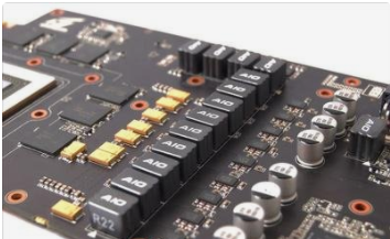
If two PCBs are to be connected with each other, we usually use the edge connector commonly known as "golden finger". The gold finger contains many bare copper pads, which are actually part of PCB wiring. Usually, when connecting, we insert the golden finger on one PCB into the appropriate slot on the other PCB (generally called expansion slot Slot).
In computers, such as display cards, sound cards or other SIMilar interface cards, are connected to the motherboard by means of golden fingers. Green or brown on PCB is the color of solder mask. This layer is an insulating protective layer, which can protect copper wires and prevent parts from being welded to incorrect places.
A layer of silk screen will be printed on the solder mask. Usually, words and symbols (mostly white) will be printed on it to MARK the position of each part on the board. The screen printing surface is also called the icon surface.
We just mentioned that on the most basic PCB, parts are concentrated on one side and wires are concentrated on the other side. Because the wires only appear on one side, we call this PCB single sided. Because there are many strict restrictions on the design circuit of a single panel (because there is only one side, and the wiring cannot cross and must go around a separate path), only early circuits use such boards. Double Sided Boards are circuit boards with wiring on both sides. However, if you want to use two wires, you must have a proper circuit connection between them. This "bridge" between circuits is called a pilot hole (via).
The pilot hole is a small hole filled with or coated with metal on the PCB, which can be connected with the wires on both sides. Because the area of the double-sided board is twice as large as that of the single panel, and because the wiring can be staggered (it can be wound to the other side), it is more suitable for circuits more complex than the single panel.
In order to increase the area that can be wired, Multi layer boards use more single or double sided wiring boards. Several double-sided boards shall be used for multilayer boards, and a layer of insulating layer shall be placed between each layer of boards and then glued (pressed). The number of layers of the board represents several independent wiring layers. Usually, the number of layers is even and includes the two outermost layers. Most motherboards are 4-8 layer structures, but technically, nearly 100 layers of PCB can be achieved. Most large supercomputers use multilayer mainboards. However, since such computers can already be replaced by clusters of many ordinary computers, super Multilayer boards have been gradually eliminated. Because the layers in the PCB are closely combined, it is generally not easy to see the actual number. However, if you carefully observe the motherboard, you may see it.
If the guide hole (via) we just mentioned is applied to the double-sided board, it must pierce the whole board. However, in a multilayer board, if you only want to connect some of the circuits, the pilot hole may waste some circuit space in other layers. Buried vias and Blind vias can avoid this problem because they only penetrate several layers. The blind hole is used to connect several layers of internal PCBs and surface PCBs without penetrating the whole board. The embedded hole is only connected to the internal PCB, so it cannot be seen from the surface. In a multilayer PCB, the whole layer is directly connected to the ground wire and power supply. So we classify each layer as signal layer, power layer or ground layer.
If parts on a PCB need different power supplies, such PCBs usually have more than two layers of power and wire layers. Part packaging technology Plug in packaging technology places parts on one side of the board and welds the pins on the other side. This technology is called "Through Hole Technology (THT)" packaging. This type of part will take up a lot of space, and will need to drill a hole for each joint pin. So their pins actually take up space on both sides, and the solder joints are relatively large. On the other hand, THT parts are better connected with PCBs than SMT (Surface Mounted Technology) parts. We will talk about this later.
For example, flat cable sockets and similar interfaces need to be pressure resistant, so they are usually THT packaged.
surface mounted Technology (SMT) uses surface mounted technology (SMT) parts, and the pins are welded on the same side as the parts. This technology does not need to weld each pin, but drill holes in PCB.
Surface adhesive parts can even be welded on both sides. SMT is also smaller than THT parts. Compared with PCBs using THT parts, PCBs using SMT technology are much denser. SMT package parts are also cheaper than THT's. Therefore, it is not surprising that most of today's PCBs are SMTs. Because the solder joints and the pins of the parts are very small, it is very difficult to use manual welding. However, if we consider that the current assembly is fully automatic, most of this problem will only occur when repairing parts.
26 Common Terms in PCB Design
10-23,2022


抖音二維碼

Q Q二維碼

微信二維碼
點(diǎn)擊
然后
聯(lián)系
然后
聯(lián)系
電話熱線
13410863085Q Q

微信

- 郵箱