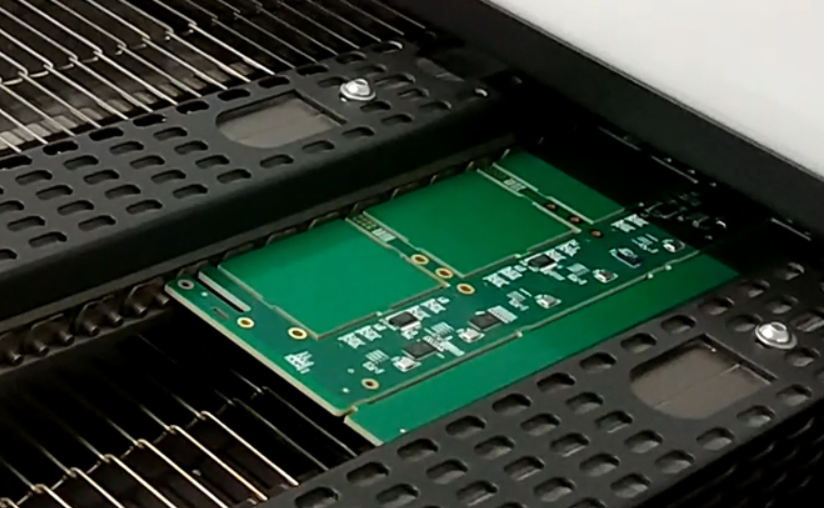

At the beginning of the new design, most of the time was spent on circuit design and component selection. At the PCB layout stage, due to lack of experience, the consideration was not comprehensive enough. If suffICient time and effort are not provided for PCB layout design, problems may occur in the manufacturing phase or functional defects may occur when the design is converted from digital domain to physical reality. So, what is the key to designing a circuit board that is real and reliable both on paper and in physical form? Let's discuss how to design a printable and reliable PCB.

First, fine tune your component layout
In the component placement stage of PCB layout process, it is both scientific and artistic, and the main components available on the circuit board need to be strategically considered. Although this process can be challenging, the way you place the electronIC components will determine how easy it is to make a circuit board and how it meets your initial design requirements.
Although there is a general order for placing components, such as placing connectors, installing components on printed circuit boards, power circuits, precision circuits, key circuits, etc. In order, there are some specific rules to remember, including:
Orientation - Ensure that SIMilar components are positioned in the same direction, which will help achieve an efficient and error free welding process.
Layout - Avoid placing SMAller components behind larger components, which may cause installation problems due to welding larger components.
Organization - It is recommended that all surface mount (SMT) components be placed on the same side of the board and all through hole (th) components be placed on the top of the board to minimize assembly steps.
Finally, we need to pay attention to a PCB design guideline - that is, when using hybrid technology components (via and surface mount components), manufacturers may need additional processes to assemble circuit boards, which will increase your overall cost.
Good chip module direction (left) and bad chip module direction (right)
Good chip module direction (left) and bad chip module direction (right)
Good component arrangement (left) and poor component arrangement (right)
Good component arrangement (left) and poor component arrangement (right)
Secondly, correctly place the power supply, grounding and signal routing
After placing components, you can place power, ground, and signal wiring to ensure that the signal path is clean and fault free. At this stage of the layout process, remember the following guidelines:
Locate power and ground plane
It is always recommended to place the power and ground layers inside the circuit board while maintaining symmetry and centering. This helps prevent your circuit board from bending, which is also related to whether your components are correctly positioned. In order to supply power to the integrated circuit, it is recommended to use a common channel for each power supply to ensure that the wiring width is firm and stable, and avoid daisy chain power connection between components.
Signal line wiring connection
Next, connect the signal line according to the design in the schematic diagram. It is recommended to always take the shortest possible path and direct path routing between components. If your components need to be fixed in the horizontal direction without any deviation, it is recommended that the components of the circuit board are basically laid horizontally at the socket, and then laid vertically behind the socket. In this way, with the migration of solder during welding, the component will be fixed in the horizontal direction. As shown in the upper part of the figure below. However, the signal routing mode in the lower part of the figure below may cause the components to deflect with the solder flow during PCB welding.
Suggested wiring method (arrow indicates solder flow direction)
Suggested wiring method (arrow indicates solder flow direction)
Unsupported wire connection mode (arrow indicates solder flow direction)
Unsupported wire connection mode (arrow indicates solder flow direction)
Define network width
Your design may require different networks that will carry various currents that will determine the required network width. Considering this basic requirement, it is recommended to provide 0.010 "(10mil) width for low current analog and digital signals. When your line current exceeds 0.3A, it should be widened. Here is a free line width calculator to make the conversion process simple.
Third, effective isolation
You may have experienced how high voltage and current SPIkes in the power circuit can interfere with your low-voltage current control circuit. To minimize such interference problems, follow these guidelines:
Isolation - Ensure that the power ground and control ground for each power supply are separate. If you must connect them together on the printed circuit board, make sure it is as close to the end of the power path as possible.
Layout - If you have placed a ground plane in the middle layer, be sure to place a small impedance path to reduce the risk of interference from any power circuit and help protect your control signal. You can follow the same guidelines to separate digital and analog grounding.
Coupling - In order to reduce the capacitive coupling of the large ground plane and its upper and lower wiring, try to pass through the analog ground only through the analog signal wire.
Example of component isolation (digital and analog)
Example of component isolation (digital and analog)
Fourth, solve the heat problem
Have you ever experienced circuit performance degradation or even circuit board damage due to heat dissipation problems? Because heat dissipation is not considered, many problems perplex many designers. Here are some guidelines to help solve cooling problems:
Identify problematic components
The first step is to start to consider which components on the circuit board have the most heat dissipation. This can be achieved by first finding the "thermal resistance" rating in the device's data book, and then transferring the generated heat according to the recommended guidelines. Of course, radiators and cooling fans can be added to keep the temperature of components down, and remember to keep key components away from any high heat source.
然后
聯(lián)系
電話熱線
13410863085Q Q

微信

- 郵箱


