鑫景福致力于滿足“快速服務,零缺陷,輔助研發”PCBA訂購單需求。


PCBA方案設計
1. What problems should be paid attention to in high-frequency signal wiring?
The signal line; Space isolation and other signal lines; For digital high-frequency signal, the differential line will be better.
2. When wiring the circuit board, if the lines are dense, there may be more holes. Of course, this will affect how to improve the electrICal performance of the PCB?

For low-frequency signals, vias do not matter. For high-frequency signals, vias should be minimized. If there are many circuits, consider multilayer boards.
3. Is it true that the more decoupling capacitors added to PCB, the better?
The decoupling capacitor needs to add the appropriate value at the appropriate position. For example, in the power port of ADI, it needs to be added. Stray signals with different frequencies need to be filtered by capacitance values.
4. What is the standard of a good PCB?
PCB layout is reasonable, power line power redundancy is sufficient, high frequency impedance and low frequency routing are SIMple.
5. How do PCB through-hole and blind hole affect the difference of signals? Apply principles What?
Blind holes or embedded holes are used to increase the density of multilayer plates, reduce the number of layers, and effectively reduce the number of plated through holes. However, by contrast, through holes are well implemented in the process and have low cost, so they are used in general PCB design.
6. When it coMES to analog digital hybrid system, it is recommended to do electrical layering.
Cut, the whole ground plane is copper plated, and it is also recommended to divide the electric layer. Different grounding connections are at the power supply end, but the return path of the signal is far. How to choose the appropriate method for specific applications?
This article: If there are high frequency 20 MHz signal lines, and the length and number exceed in addition, the analog high frequency signal requires at least two layers. The letter line 1 on the first floor has a large area on the first floor, and the signal line floor needs to be grounded with enough vias. The purpose of this is to provide complete transmission medium and impedance matching for analog signals; The ground plane isolates the analog signal from other digital signals. The ground circuit is SMAll enough, because you have made many holes, and the ground is a big flat noodles.
7. On the pcb circuit board, the signal input plug-in is on the leftmost edge of the PCB, the MCU is on the right, and the stable power supply chip is placed at the connector near the source during the layout process (the output 5V of the power supply IC arrives after a long path. Single chip computer), or the power supply IC is placed on the right side of the middle (the output 5V line of the power supply IC arrives at the single chip computer shorter, but the input power line segment is longer)? Or is there a better layout?
1、 Is the signal input plug-in an analog device? For analog devices, it is recommended that the power supply layout should not affect the signal straightness of the analog part as much as possible. Therefore, there are several points to consider: First of all, is the regulated power supply chip a clean power supply with small ripple? The power supply of the proposed part of the mode requires high power supply; Is the analog part and the single-chip microcomputer the power supply in the high-precision circuit? In PCB design, it is recommended to separate the power supply of analog part and digital part; The power supply of the digital part needs to minimize the influence of the power supply of the analog circuit part.
8. In the application of high-speed signal chain, multiple ASICs have analog land and digital land. Are they divided or not? What are the existing standards? Which effect is better? This article: So far there is no final conclusion. Generally speaking, you can refer to the chip manual. Grounding is recommended in all ADI hybrid chip manuals. Public land is recommended for some schemes, and independent land is recommended for some schemes
Two signal lines? What is the maximum length difference of? Calculate?
Difference line calculation idea: if the sine signal is transmitted, the length is different and equal to half of its transmission wavelength, the phase difference is 180 degrees, and then the 2 degree signal is completely canceLED. So the length difference is the largest at this time. By analogy, the difference between signal lines is to ensure that the value is less than this value.
10. What kind of situation is the serpentine route suitable for at high speed? What are the disadvantages? For example, for differential routing, two sets of signals are required to be orthogonal. Serpentine wiring has different functions due to different applications
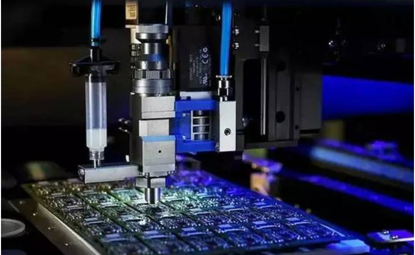
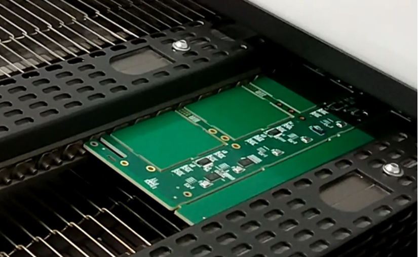
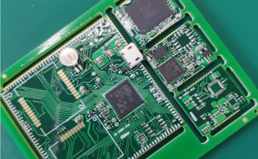
In this article, it is mainly about the introduction of PCB design and wiring knowledge literacy in the PCB manufacturing process


抖音二維碼

Q Q二維碼

微信二維碼
點擊
然后
聯系
然后
聯系
電話熱線
13410863085Q Q

微信

- 郵箱