鑫景福致力于滿足“快速服務,零缺陷,輔助研發”PCBA訂購單需求。


PCBA方案設計

General PCB basIC design process is as follows:
Preliminary preparation → PCB structure design → guide network table → rule setting → PCB layout → wiring → wiring optimization and silk screen printing → network and DRC inspection and structure inspection → output photo drawing → photo drawing review → PCB board making production/proofing data → PCB board factory engineering EQ confirmation → chip mounting data output → project completion.
1: Preliminary preparation
This includes preparing package libraries and schematICs. Before PCB design, first prepare the logic package of schematic SCH and the package library of PCB. The package library can be the library provided with PADS, but it is difficult to find a suitable one in general. It is better to make your own package library according to the standard size information of the selected components. In principle, the packaging library of PCB shall be built first, and then the logic packaging of SCH shall be built. PCB packaging library has high requirements, which directly affects the installation of boards; The logic packaging requirements of SCH are relatively loose. Just pay attention to defining the pin attributes and the corresponding relationship with PCB packaging. PS: Note the hidden pins in the standard library. After that, it is the schematic design. After that, it is ready to start PCB design.
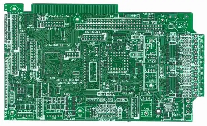
2: PCB structure design
In this step, the PCB surface is drawn in the PCB design environment according to the determined PCB size and various mechanical positioning, and the required connectors, keys/switches, screw holes, assembly holes, etc. are placed according to the positioning requirements. And fully consider and determine the wiring area and non wiring area (such as how large the area around the screw hole belongs to the non wiring area).
3: Guide net list
It is recommended to import the board frame before the net guide table. Import fraMES in DXF format or emn format.
4: Rule Settings
Reasonable rules can be set according to the specific PCB design. What we call the rules is the constraint manager of PADS. The constraint manager restricts the line width and safety spacing at any link in the design process. The DRC MARKers will be used to mark the areas that do not meet the constraints during subsequent DRC detection.
The general rule setting is placed before the layout because sometimes it is necessary to complete some fanout work during the layout. Therefore, the rules should be set before fanout. When the design project is large, the design can be completed more efficiently.
Note: Rules are set for better and faster design, in other words, for the convenience of designers.
General settings are:
1. Default line width/line spacing of common signal.
2. Select and set vias
3. Line width and color setting of important signals and power supplies.
4. Plate layer setting.
5: PCB layout
The general layout shall follow the following principles:
(1) According to the reasonable division of electrical performance, it is generally divided into: digital circuit area (i.e., fear of interference and generate interference), analog circuit area (fear of interference), power drive area (interference source);
(2) Circuits that complete the same function shall be placed as close as possible, and all components shall be adjusted to ensure the most concise connection; At the same time, adjust the relative position between the function blocks to make the connection between the function blocks the most concise;
(3) For components with high quality, the installation position and strength shall be considered; The heating element shall be placed separately from the temperature sensing element, and thermal convection measures shall be considered when necessary;
(4) The I/O driver shall be close to the edge of the printed board and the outlet connector as far as possible;
(5) The clock generator (such as crystal oscillator or clock oscillator) shall be as close as possible to the device using the clock;
(6) A decoupling capacitor shall be added between the power input pin of each integrated circuit and the ground (generally, a monolithic capacitor with good high-frequency performance is used); When the circuit board space is dense, a tantalum capacitor can also be added around several integrated circuits.
(7) Discharge diode (1N4148) shall be added at relay coil;
(8) The layout should be balanced, dense and orderly, not top heavy or heavy.
Special attention shall be paid to the actual size (area and height) of components and the relative position between components when placing components, so as to ensure the electrical performance of the circuit board and the feasibility and convenience of production and installation. At the same time, the placement of components shall be properly modified to make them neat and beautiful on the prEMIse that the above principles can be reflected. SIMilar components shall be placed orderly and in the same direction, It should not be placed in an "orderly manner".
This step is related to the overall image of the board and the difficulty of wiring in the next step, so we should make great efforts to consider it. In the layout, preliminary wiring can be made for uncertain places, and full consideration can be given.


抖音二維碼

Q Q二維碼

微信二維碼
點擊
然后
聯系
然后
聯系
電話熱線
13410863085Q Q

微信

- 郵箱