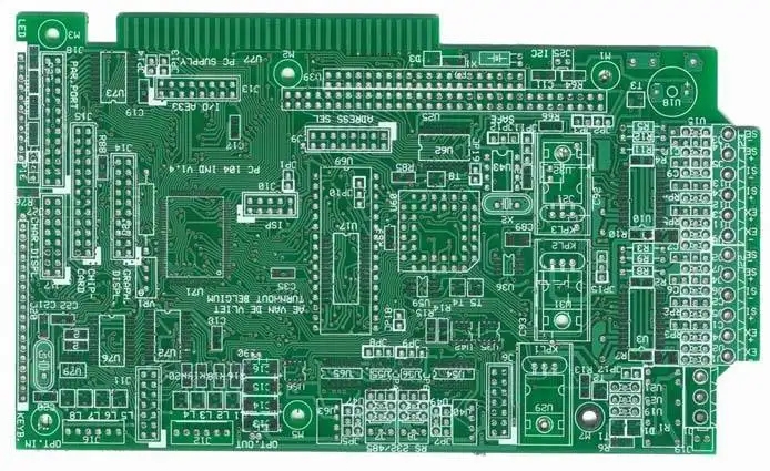
鑫景福致力于滿足“快速服務,零缺陷,輔助研發”PCBA訂購單需求。


PCBA方案設計
6: Wiring
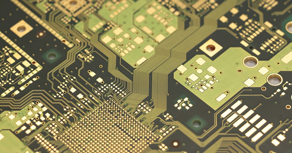
Wiring is the most important process in PCB design. This will directly affect the performance of PCB. In the PCB design process, there are generally three levels of wiring:
The first is wiring, whICh is the most basic requirement for PCB design. If the lines are not connected and there are flying lines everywhere, it will be an unqualified board. It can be said that we haven't started yet.
The second is the satisfaction of electrical performance. This is the standard to measure whether a printed circuit board is qualified. This is to carefully adjust the wiring after wiring to achieve the best electrical performance.
Next is beauty. If your wiring is connected, there is no place that affects the performance of electrical appliances. But at a glance, it is chaotic, colorful and colorful. Even if your electrical performance is good, it is still a piece of garbage in the eyes of others. This brings great inconvenience to testing and maintenance. The wiring shall be neat and uniform, and shall not be crisscross and disorganized. All these should be achieved under the prEMIse of ensuring the electrical performance and meeting other individual requirements, otherwise, it will be a waste of time.
The wiring shall be carried out according to the following principles:
(1) In general, the power line and ground wire shall be wired first to ensure the electrical performance of the circuit board. Within the allowable range, the width of power supply and ground wire shall be widened as much as possible. The ground wire is better than the power wire. Their relationship is: ground wire>power wire>signal wire. Generally, the width of signal wire is 0.2 ~ 0.3mm (about 8-12mil), the thinnest width can reach 0.05 ~ 0.07mm (2-3mil), and the power wire is 1.2 ~ 2.5mm (50-100mil). The PCB of digital circuit can be used to form a loop with a wide ground wire, that is, to form a ground grid for use (the ground of analog circuit cannot be used in this way).
(2) Wires with strict requirements (such as high-frequency lines) shall be wired in advance. The side lines of input and output terminals shall not be adjacent and parallel to each other to avoid reflection interference. If necessary, ground wires shall be added for isolation, and the wiring of two adjacent layers shall be perpendicular to each other, which may cause parasitic coupling.
(3) The oscillator shell shall be grounded, and the clock line shall be as short as possible, and shall not be LED everywhere. The area of the ground under the clock oscillation circuit and special high-speed logic circuit should be added, and other signal lines should not be used to make the surrounding electric field approach zero;
(4) 45 ° broken lines shall be used as far as possible, and 90 ° broken lines shall not be used to reduce the radiation of high-frequency signals; (Double arc lines are also used for lines with high requirements)
(5) No signal line shall form a loop. If it is unavoidable, the loop shall be as SMAll as possible; The vias of signal lines shall be as few as possible;
(6) The key lines shall be as short and thick as possible, and protective areas shall be added on both sides.
(7) When transmitting sensitive signals and noise field band signals through flat cables, they should be led out in the way of "ground wire signal ground wire".
(8) Test points shall be reserved for key signals to facilitate production, maintenance and detection
(9) After the schematic wiring is completed, the wiring shall be optimized; At the same time, after the preliminary network inspection and DRC inspection are correct, fill the ground wire in the unrouted area, use a large area of copper layer as the ground wire, and connect the unused places with the ground on the printed board as the ground wire. Or it can be made into multilayer boards, with one layer for power supply and one layer for ground wire.
PCB wiring process requirements (can be set in rules)
(1) Line
In general, the signal line width is 0.3mm (12mil), and the power line width is 0.77mm (30mil) or 1.27mm (50mil); The distance between lines and between lines and pads shall be greater than or equal to 0.33mm (13mil). In practical application, if conditions permit, the distance shall be increased;
When the wiring density is high, it can be considered (but not recommended) to use two lines between IC pins, the width of the line is 0.254mm (10mil), and the line spacing is not less than 0.254mm (10mil). Under special circumstances, when the device pins are dense and the width is narrow, the line width and line spacing can be appropriately reduced.
(2) Pads
The basic requirements for PAD and VIA are: the diameter of PAD is greater than that of hole by 0.6 mm; For example, universal pin resistors, capacitors, integrated circuits, etc., adopt 1.6mm/0.8mm (63mil/32mil) disk/hole size, 1.8mm/1.0mm (71mil/39mil) socket, pin, diode 1N4007, etc. In practical application, it shall be determined according to the size of the actual component. If possible, the pad size can be appropriately increased;
The component installation hole diameter designed on the PCB shall be 0.2~0.4mm (8-16mil) larger than the actual size of the component pin.
(3) Via (VIA)
Generally 1.27mm/0.7mm (50mil/28mil);
When the wiring density is high, the via size can be appropriately reduced, but should not be too small, and 1.0mm/0.6mm (40mil/24mil) can be considered.
(4) Spacing requirements for pads, wires and vias
PAD and VIA :≥ 0.3mm(12mil)
PAD and PAD :≥ 0.3mm(12mil)
PAD and TRACK :≥ 0.3mm(12mil)
TRACK and TRACK :≥ 0.3mm(12mil)
When the density is high:
PAD and VIA :≥ 0.254mm(10mil)
PAD and PAD :≥ 0.254mm(10mil)
PAD and TRACK :≥ 0.254mm(10mil)
TRACK and TRACK :≥ 0.254mm(10mil)
7: Routing optimization and silk screen
"There is no best, only better"! No matter how hard you try to design, after you finish painting, you will still feel that there are many places that can be modified. The general design experience is that the time for optimal routing is twice as long as the time for initial routing. I don't think there is anything that needs to be modified. After that, I can lay copper. Copper is generally laid with ground wire (pay attention to the separation of analog ground and digital ground), and power supply may also be required for multi-layer boards. For silk screen, it should be noted that it cannot be blocked by devices or removed by vias and pads. At the same time, when designing, face up to the component surface, and the characters at the bottom layer should be mirrored to avoid confusing the layers.
8: Network, DRC check and structure check
Before photo painting, it is generally necessary to check. Each company will have its own Check List, which contains the requirements of principle, design, production and other aspects. The following describes the two main inspection functions provided by the software.
9: Output photo
Before the photo output, it is necessary to ensure that the veneer is the latest version that has been completed and meets the design requirements. The photo output files are used for plate making in the plate factory, steel MESh making in the steel mesh factory, welding process documents in the welding factory, etc.
The output files are:
1). Wiring layer: refers to the conventional signal layer, mainly wiring.
It is named L1, L2, L3, L4, where L represents the layer of the routing layer.
2). Silk screen layer: refers to the layer in the design document that provides information for processing silk screen. Generally, if there are devices or MARKs on the top and bottom layers, there will be top and bottom silk screen.
Naming: the top layer is named SILK_ TOP ; The underlying layer is named SILK_ BOTTOM 。
3). Soldering resistance layer: refers to the layer in the design document that provides processing information for green oil coating.
Naming: the top layer is named SOLD_ TOP; The underlying layer is named SOLD_ BOTTOM。
4). Steel mesh layer: refers to the layer in the design document that provides processing information for solder paste coating. Generally, when there are SMD devices on the top layer and bottom layer, there will be steel mesh top layer and steel mesh bottom layer.
Naming: the top layer is named PASTE_ TOP ; The underlying layer is named PASTE_ BOTTOM。
5). Drilling layer (including 2 files, NC DRILL NC drilling file and DRILL DRAWINGdrilling map)
They are named NC DRILL and DRILL DRAWINGrespectively.
10: Photo examination
After outputting photo, photo inspection, CAM350 open short circuit and other inspections should be carried out before sending it to the plate factory for plate making. In the later stage, attention should be paid to the plate making engineering and problem reply.
11: PCB board making data (Gerber photo drawing data+PCB board making requirements+assembly drawing)
12: PCB factory engineering EQ confirmation (board making engineering and question reply)
13: PCBA patch data output (steel grid data, patch tag number diagram, component coordinate file)
At this point, all the workflow of PCB design for a project is completed
PCB design is a very meticulous work, so we should be extremely careful and patient in design, and fully consider all factors, including production, assembly and processing, and ease of maintenance in the later period. In addition, develop some good work habits during design, which will make your design more reasonable, design more efficient, production easier, and performance better. When good design is applied to daily products, consumers will feel more confident and trust.
Introduction of pcb design drawing software
10-26,2022


抖音二維碼

Q Q二維碼

微信二維碼
點擊
然后
聯系
然后
聯系
電話熱線
13410863085Q Q

微信

- 郵箱