鑫景福致力于滿足“快速服務,零缺陷,輔助研發”PCBA訂購單需求。


PCB制造
Briefly describe PCB processing flow
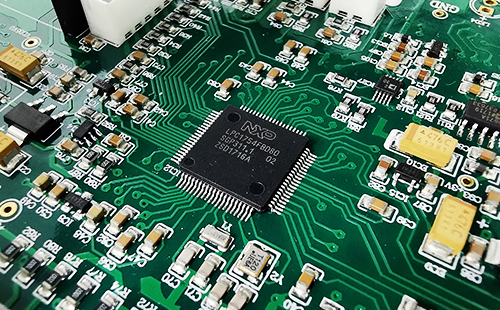
At present, in the field of electronIC product processing, PCB as one of the important electronIC components is indispensable. At present, there are many types of PCB, such as high-frequency pcb boards, microwave PCB boards and other kinds of printed circuit boards have made a certain reputation in the MARKet. PCB manufacturers have specific processing and manufacturing processes for various types of boards. But generally speaking, three aspects need to be considered when PCB board is processed.
1. Consider the selection of base materials
PCB substrate can be divided into organic materials and inorganic materials. Each material has its unique advantages. Therefore, dielectric property, copper foil type, base slot thickness, machinability and other properties are considered when determining the type of substrate. Among them, the thickness of the surface copper foil is the key factor affecting the performance of this PCB. Generally speaking, the thinner the thickness is, the more convenient the etching is and the higher the precision of the pattern is.
2. Consider the setting of production environment
The environment of PCB processing and manufacturing workshop is also a very important aspect, and the regulation and control of environmental temperature and humidity are crucial factors. If the ambient temperature changes too significantly, it may cause the drilling hole on the base material plate to break. If the ambient humidity is too high, nuclear energy will adversely affect the performance of the substrate with strong water absorption, specifically in terms of dielectric properties. Therefore, it is necessary to maintain appropriate environmental conditions during PCB board processing and production.
3. Consider the selection of process flow
The production of PCB is easily affected by many factors. The processing layers, punching process, surface coating treatment and other processes will affect the quality of PCB finished products. Therefore, for these process flow environments, the processing and manufacturing of PCB boards are fully considered in combination with the characteristics of the manufacturing equipment, and can be flexibly adjusted according to the different types of pcb boards and processing needs.
To sum up, the selection of base materials, the setting of production environment and the selection of process flow should be considered when pcb boards are processed. At the same time, the processing and blanking method of PCB engineering materials is also an aspect that needs to be carefully selected, which is closely related to the layout smoothness of the finished PCB.
Many engineers or customers have not seen the PCB processing process at the PCB processing plant. Today, I will SIMply tell you about the PCB processing process, so that you can have a general impression of the PCB processing process.
1. Material opening
Cutting the raw materials of CCL into the size we need is calLED cutting. The opening process is to improve the utilization of raw materials and reduce the price of veneer.
2. Pretreatment
Remove the pollutants on the copper surface, increase the roughness of the copper surface, and facilitate the later film pressing process.
3. Pressing film
The treated copper surface of the substrate is pasted with an anti-corrosion dry film by hot pressing.
4. Exposure
The image on the original negative is transferred to the photosensitive base plate through the light irradiation.
5. Development
The dry film without chEMIcal reaction is washed away by the action of alkali solution, while the dry film with reaction is left on the board as the anti-corrosion protective layer for etching.
6. Etching
The copper exposed after development is etched with the solution to form the inner layer circuit pattern.
7. Demembrane
The strong alkali is used to peel the corrosion resistant layer of the protective copper surface to expose the line pattern.
8. Punching
Punch out the positioning hole and rivet hole with CCD.
9. AOI inspection
Through automatic optical inspection, compare with the sample or original data to find defects.
10. Drilling
Drill through holes for connecting lines between layers on the pcb board.
11. Copperplate
Remove the burr on the edge of the hole to prevent poor hole plating.
12. Electroplating
Electrolysis is used to prevent metal oxidation and improve wear resistance and conductivity.
13. Resistance welding
Leave the parts to be welded on the PCB, and cover other lines and copper surfaces to improve electrical performance.
14. Silk screen
It is convenient for circuit maintenance and installation, and the sign pattern and letter code are used for annotation.
15. Surface treatment
In order to better welding reliability, thermal stability and surface smoothness, the surface treatment of PCB is made.
16、V-CUT
It is convenient and smooth to cut the original panel into veneer.
17. Electrical test
Perform bare board test on the electrical performance of PCB board to meet customer requirements.
All PCB boards will have the above processing flow, but different layers of PCB boards will have different processing flow tiMES.
How to quickly judge the quality of PCB
10-27,2022


抖音二維碼

Q Q二維碼

微信二維碼
點擊
然后
聯系
然后
聯系
電話熱線
13410863085Q Q

微信

- 郵箱