鑫景福致力于滿足“快速服務,零缺陷,輔助研發”PCBA訂購單需求。


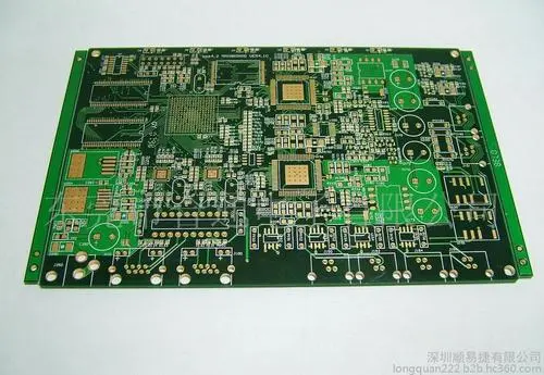
PCB制造
It should be noted that the number of cabling layers, grounding planes and power supply planes required to achieve the required functions of the circuit is related to the basIC functions of the circuit, signal integrity, EMI, EMC, manufacturing costs, etc.
Compared with most designs, there are many conflicting requirements for key factors such as performance requirements, cost, manufacturing technology and system complexity of PCB. Generally speaking, the stack design of PCB is a compromise after considering key factors in all aspects. In general, high-speed digital circuits and RF circuits are designed with multilayer boards.
layered
In multilayer PCB circuit boards, there are usually signals, power planes and ground planes. The power plane and the grounding plane are generally undivided solid planes. They will provide a good current return path with low impedance for the current of adjacent signal lines.
The signal layer is mostly located between such power or ground reference plane layers, forming symmetric striplines or asymmetric striplines. The top and bottom layers of multilayer PCB circuit boards are generally used to prevent PCB components and a SMAll amount of wiring. The wiring of such signals should not be too long to reduce the direct radiation caused by wiring.
Determine single power reference plane
Safe use of decoupling capacitors is a crucial measure to deal with power integrity. Decoupling capacitors can only be stored on the top and bottom layers of PCB.
PCB routing, PCB pad and via of decoupling capacitor will seriously affect the effect of decoupling capacitor. Therefore, the wiring connecting the decoupling capacitor must be fully considered in the design, which should be as short and wide as possible, and the wire connected to the via should also be as short as possible.
Determine the multi power reference plane
The multi power reference plane will be divided into several solid areas with different voltages. If the signal layer is next to the multiple power supply layer, the signal current on the signal layer nearby may suffer from an unsatisfactory return path, resulting in gaps in the return path.
Compared with high-speed digital signals, these unreasonable return path designs may cause serious problems. Therefore, high-speed digital signal wiring is required to be far away from multiple power reference planes.
Determine multiple ground reference planes
Many ground reference planes can create a good current return path with low impedance, which can greatly reduce common mode EMI.
The ground plane and the power plane must be closely coupLED, and the signal layer must also be closely coupled with the adjacent reference plane. The thickness of the medium between layers is reduced to facilitate this purpose.
Reasonable PCB design and wiring combination
The two levels crossed by a signal path are one [wiring combination]. The most suitable PCB wiring combination design is to avoid the return current as much as possible, and flow from one reference plane to another; Instead, it is left from one point (face) of a reference plane to another point (face).
Briefly describe PCB processing flow
10-27,2022


抖音二維碼

Q Q二維碼

微信二維碼
點擊
然后
聯系
然后
聯系
電話熱線
13410863085Q Q

微信

- 郵箱