鑫景福致力于滿足“快速服務,零缺陷,輔助研發”PCBA訂購單需求。


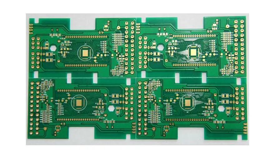
PCB制造

Perforated copper plating for PCB electroplating
The main feature of the electroporation copper plating processing technology used by circuit board manufacturers to produce multilayer impedance circuit boards is the blind hole of the mICro through hole formed in the circuit boards of multilayer PCB boards with "core boards". These micro through holes should be electroporated and copper plated to realize the electrical interconnection between layers. The key to the metallization and electroplating of such blind buried holes is the access and replacement of electroplating solution.
In the manufacturing of multilayer PCB boards, circuit board manufacturers are made by coating or laminating a dielectric layer (or coating resin copper foil) on the board surface with a "core board" and forming a micro through hole. These micro through holes formed by laminating on the "core plate" are made by methods such as photoinduced method, plaSMA method, laser method and sand blasting method (mechanical method, including numerical control drilling method not introduced). The micro through holes of multilayer pcb circuit board shall be metallized and copper plated to realize the electrical interconnection between PCB layers. This section mainly introduces the characteristics and requirements of the micro via in PCB in the process of hole forming and electroplating.
For through holes, if it is vertical hole plating, the PCB manufacturer can swing, vibrate, stir the plating solution or spray the flow in the plate making fixture (or hanger) to make the PCB produce a hydraulic difference between the two plate surfaces of the plate making. This hydraulic difference will force the plating solution into the hole and drive away the gas in the hole, so that it will be filLED in the hole. For micro holes with high thickness to diameter ratio (thickness to diameter ratio: the ratio of the thickness of the medium layer to the micro conductive hole diameter), The existence of this hydraulic pressure difference is more important, and then the drilling or electroplating is carried out. In porous electroplating, part of Cu2+ions in the plating solution in the hole will be consumed, so the concentration of Cu2+in the plating solution in the hole will become lower and lower, and the efficiency of porous or electroplating will become smaller and smaller. In addition, the effect of the plating fluid in the hole (such as the phenomenon of "laminar flow") and the uneven distribution of current density (the current density in the hole is far lower than the current density on the board), so the coating thickness at the center of the hole is always lower than that on the board. In order to reduce the difference in coating thickness, the most fundamental methods are: first, increase the flow rate of the plating solution in the hole or the number of tiMES the plating solution is exchanged in the hole per unit time (assuming that the plating solution is replaced time after time, which is actually much more complex, but this assumption can explain the problem); The second is to increase the current density in the hole, which is obviously difficult or impractical, because to increase the current density of the plating solution in the hole, it is bound to increase the current density of the plate, which will result in a greater difference between the thickness of the coating at the center of the hole and that of the plate; The third is to reduce the current density during electroplating and the concentration of Cu2+ions in the plating solution, and at the same time increase the flow rate of the plating solution in the hole (or the number of bath exchanges). In this way, the difference in the concentration of Cu2+ions in the plating solution between the plate and the hole can be reduced (referring to the difference in the concentration of Cu2+caused by the difference between the partial consumption of Cu2+and the change of the plating solution). This measure and method can improve the difference between the thickness of the plate coating and the coating (at the center) in the hole, However, PCB productivity (output) is often sacrificed, which is undesirable; Fourth, pulse electroplating method is adopted. According to the micro via with different high thickness diameter ratio, the corresponding pulse current electroplating method {can significantly improve the difference between the coating thickness on the PCB surface and the coating thickness in the hole, or even reach the same coating thickness. Can these measures be applied to the porous electroplating of micro via in multilayer PCB?
As mentioned above, the hole plating of the micro through hole in the multilayer circuit board is carried out in the blind hole. When the hole depth of the blind hole is small or the thickness diameter ratio is small, practice has shown that the above four plating measures can achieve good results. However, when the blind hole depth is high or the thickness diameter ratio is large, what is the reliability of the porous plating of the micro through hole? In other words, how to control the proper depth or thickness diameter ratio of the blind hole of the multilayer circuit board?
There is no detailed report on the processing of micro through holes in multilayer PCB boards by horizontal hole electroplating, but people can imagine that when the thickness diameter ratio on PCB boards is not large, reliable electrical interconnection can be obtained by horizontal hole electroplating. For blind via with large thickness diameter ratio, the blind via on the lower surface of the multilayer circuit board is difficult to drive away the gas in the hole, even the plating solution is difficult to enter the hole, let alone the problem of plating solution exchange in the hole, unless the board surface is turned over regularly.
To sum up, according to the above basic characteristics and principles of the drilling and electroplating processing of multilayer PCB boards, we can draw a conclusion that the horizontal drilling electroplating processing of blind through holes in multilayer PCB boards (especially those with large thickness diameter ratio, such as thickness diameter ratio>0.8) is far less effective than the vertical drilling electroplating processing.
PCB production process flow 1
10-30,2022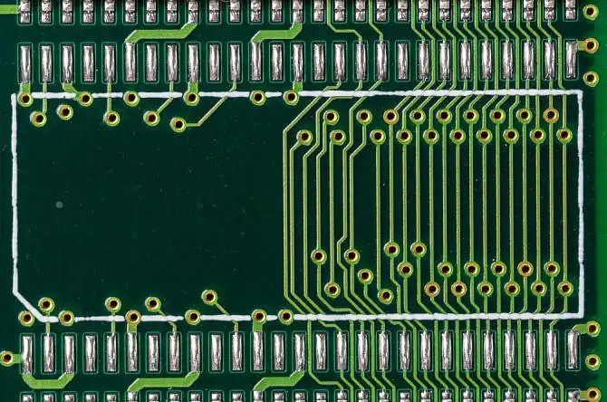


抖音二維碼

Q Q二維碼

微信二維碼
點擊
然后
聯系
然后
聯系
電話熱線
13410863085Q Q

微信

- 郵箱